In actual production and usage, warping issues in 4 layer PCBs are frequently encountered. This not only impacts production yield and assembly efficiency but also poses long-term reliability risks for end products. Upon investigating the causes of warping in 4 layer PCBs, we have identified asymmetrical lamination as the key factor contributing to this problem. This paper will subsequently analyse in detail the principles and hazards of warping in 4 layer PCBs caused by asymmetric laminations, proposing corresponding prevention and control measures.
Standard Laminate Structure and Core Value of 4 Layer PCBs
The classic laminate structure of 4 layer PCBs adheres to the ‘symmetry design principle’. Taking the most commonly used 1.6mm total thickness FR-4 material as an example, a typical stack-up comprises: Top signal layer (1oz copper foil) – Prepreg (Type 2116, approx. 0.11mm) – Core board (0.4mm, double-sided 1oz copper foil) – Prepreg (same specification as top layer) – Bottom signal layer (1oz copper foil). This symmetrical structure not only ensures signal integrity and achieves proper isolation between power planes and signal layers, but more crucially maintains physical stress balance.
The core value of symmetrical lamination lies in ‘bidirectional stress cancellation’. During production, 4 layer PCBs undergo multiple high-temperature processes including lamination, reflow soldering, and curing. Materials with differing thermal expansion coefficients will contract or expand accordingly. Within a symmetrical structure, the material composition and thickness distribution of upper and lower layers are identical. The stresses generated are thus equal in magnitude and opposite in direction, ultimately cancelling each other out to preserve the PCB’s flatness. 4 layer PCBs find applications across consumer electronics, industrial control systems, and automotive electronics. Whether in the precision assembly of portable devices or within the vibration-prone environments of automotive installations, stringent demands are placed upon PCB flatness. Symmetrical lamination provides the fundamental foundation for meeting these requirements.
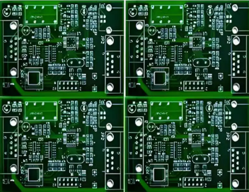
Definition and Common Manifestations of Asymmetric Laminations
Asymmetric lamination in a 4 layer PCB refers to discrepancies in material selection, thickness distribution, copper foil specifications, and prepreg combinations between upper and lower layers, resulting in the loss of mirror symmetry. This asymmetry extends beyond mere ‘uneven thickness’ to encompass ‘imbalanced mechanical properties,’ commonly manifesting in three forms:
Firstly, asymmetric material combinations, where different prepreg types are used for top and bottom layers—such as employing 1080 thin prepreg (approx. 0.07mm) on top and 7628 thick prepreg (approx. 0.18mm) on the bottom. Secondly, asymmetric copper foil thicknesses, such as using 1oz copper foil on the top layer and 2oz copper foil on the bottom layer without corresponding compensatory design. Thirdly, core board displacement occurs when the laminate structure is not symmetrically distributed around the core board, resulting in excessive differences in dielectric thickness between upper and lower layers. These seemingly minor design deviations, amplified by high-temperature processes, can trigger significant warpage issues.
Core Principles of Warpage in 4 Layer PCBs Due to Asymmetric Laminating
1.Stress Imbalance Induced by Thermal Expansion Coefficient Differences
The core materials of a PCB (copper foil, prepreg, core board) exhibit markedly different coefficients of thermal expansion (CTE): copper foil has a CTE of approximately 17 ppm/°C, while FR-4 core boards and prepregs have CTEs of around 13–15 ppm/°C (longitudinal) and 25–30 ppm/°C During lamination, PCBs endure temperatures around 180°C. Materials expand with rising temperatures and contract during cooling and curing.
In symmetrical lamination, the combined CTEs of upper and lower layers are consistent. Their contraction rates and magnitudes are perfectly symmetrical, causing thermal stresses to cancel each other out, thus maintaining PCB flatness. Asymmetric lamination disrupts this equilibrium: for instance, a top layer comprising thin prepreg + thin copper foil paired with a bottom layer of thick prepreg + thick copper foil. During cooling, the contraction of the bottom copper foil and prepreg exceeds that of the top layer. This generates inward tensile forces in the bottom layer, which the insufficient contraction of the top layer cannot counteract. Consequently, the PCB warps and bends towards the top layer. This stress imbalance does not occur instantaneously but accumulates progressively during cooling and curing, resulting in permanent warping deformation.
2.Compound Effect of Resin Flow Inhomogeneity and Curing Shrinkage Variation
As the interlayer bonding material in 4 layer PCBs, prepreg melts and flows under high-temperature lamination, filling interlayer voids before curing. In symmetrical laminations, upper and lower prepreg layers share identical resin content and flow characteristics. Under identical temperature and pressure conditions, resin flows uniformly with identical curing shrinkage rates, yielding no additional stresses.
However, asymmetric stacking—where upper and lower SMC layers differ in type or quantity—introduces variations in resin content and flowability: thicker SMCs possess higher resin content, flow over greater distances, and exhibit slightly higher curing shrinkage than thinner variants. During lamination, this disparity in resin flow velocity creates localised pressure imbalances. Post-curing, differing shrinkage rates further exacerbate stress accumulation. For instance, using one 1080 prepreg sheet for the top layer and two 1080 prepreg sheets for the bottom layer results in greater resin shrinkage in the lower layer. This induces PCB bending towards the bottom layer, causing warpage. When combined with thermal expansion stresses, this effect significantly amplifies warpage severity.
3.Mechanical Impact of Uneven Copper Foil Distribution
As the conductive medium in 4 layer PCBs, copper foil possesses inherent mechanical strength. Its uniform distribution directly influences the PCB’s overall mechanical equilibrium. The inner layer copper foil (core board surface) and outer layer copper foil collectively form the mechanical support structure. Symmetrical distribution ensures the tensile strength and shrinkage characteristics of the copper foil complement each other, maintaining structural stability.
Asymmetric lamination resulting in copper foil thickness variations or uneven distribution disrupts this mechanical equilibrium. Greater foil thickness correlates with higher tensile strength, generating increased tensile forces during shrinkage. For instance, if the top layer copper foil is 1oz (35μm) and the bottom layer is 2oz (70μm), with asymmetrical inner layer copper foil distribution, the contraction tension from the thicker bottom layer during cooling and curing will far exceed that of the thinner top layer. This forces the PCB to warp towards the top layer. Furthermore, asymmetric copper pattern density exacerbates warpage—where the bottom layer exhibits higher copper coverage than the top layer. This creates greater contraction resistance in the bottom layer, resulting in smaller contraction than the top layer and causing the PCB to bend towards the bottom layer.
Hazards of Asymmetric Laminating Warpage in 4 Layer PCBs
1.Direct Impact on Production and Assembly
Warped 4 layer PCBs directly reduce production yield rates. During the SMT placement process, warped PCBs fail to align precisely with the stencil, leading to uneven solder paste printing, insufficient solder, or solder bridging. This subsequently causes cold solder joints and short circuits. During through-hole assembly, warped PCBs fail to insert smoothly into slots. Forced assembly risks PCB fracture and component damage. Furthermore, uneven heating during reflow soldering exacerbates warping, creating a vicious cycle.
For mass production, while mildly warped PCBs may be rectified through correction processes, this increases production costs and cycle times. Severely warped PCBs are scrapped outright, resulting in material waste and delivery delays. Industry data indicates that warping defects in 4 layer PCBs caused by asymmetric lamination can reach defect rates as high as 8%-12%, significantly impacting corporate profitability.
2.Long-term reliability risks for end products
Even if warped 4 layer PCBs are successfully assembled after correction, they introduce enduring reliability hazards for end products. During operation, environmental temperature fluctuations and vibration/shock gradually release accumulated internal stresses, causing warpage recurrence. This tension strains solder joints, inducing fatigue and detachment, ultimately triggering equipment failure.
This vulnerability becomes more pronounced in specific application scenarios: – In automotive electronics subjected to temperature cycling (-40°C to 85°C) and vibration, solder joint failure rates on warped PCBs are 3-5 times higher than on flat PCBs; In industrial control equipment during prolonged operation, warp-induced deformation of signal layers disrupts impedance matching, causing signal attenuation and heightened electromagnetic interference; In consumer electronics like smartphones, where space is compact, warped PCBs may compress batteries or screens, creating safety hazards.
Key Considerations for Symmetrical Laminate Design and Warpage Control in 4 Layer PCBs
1.Core Design Principles: Mirror Symmetry and Mechanical Equilibrium
The laminate design for 4 layer PCBs must strictly adhere to the principle of ‘mirror symmetry’. Centred on the core board, the material composition, thickness distribution, and copper foil specifications of the upper and lower layers must be perfectly symmetrical. For instance, if the core board is 0.4mm thick with a top layer of ‘1oz copper foil + 1 sheet of 2116 prepreg’, the bottom layer must correspondingly use ‘1oz copper foil + 1 sheet of 2116 prepreg’ to ensure identical thermal expansion and curing shrinkage characteristics.
Should prepreg thickness require adjustment for impedance control, a ‘symmetrical compensation’ design must be employed: adding one sheet of 1080 prepreg to the top layer necessitates adding one sheet of the same specification to the bottom layer, or achieving balance by adjusting the dielectric thickness on either side of the core board. Regarding copper foil design, the thickness of copper foil on both layers must remain consistent. Should significant variations in inner layer copper density occur, compensate by adjusting the pattern density of the outer layer copper foil to maintain overall mechanical equilibrium.
2.Collaborative Control of Material Selection and Process Parameters
Material selection must balance consistency and compatibility. Prioritise using prepregs and core boards from the same batch and model to ensure uniformity in parameters such as thermal expansion coefficient and resin content. Avoid mixing materials from different manufacturers or batches to minimise stress imbalances caused by material property variations.
Process parameter optimisation aids warpage control: employ a ‘gradual heating, stepwise pressure application’ mode during lamination, with a heating rate controlled at 2°C/min to prevent uneven resin flow from abrupt temperature rises. During cooling, implement a gradual descent at 1°C/min to allow sufficient stress release time. Additionally, pre-bake treatment (120°C for 2 hours) of core boards and prepregs prior to lamination removes moisture, reducing bubble formation and shrinkage variations during curing.
3.Warpage Correction and Defect Handling Procedures
For 4 layer PCBs exhibiting minor warping (warp degree 0.5–0.8 mm), employ hot-press correction: place the PCB in a hot press, maintain at 120°C under 15 kg/cm² pressure for 30 minutes, then slowly cool to room temperature. This releases internal stresses through combined external force and temperature regulation, restoring flatness. For PCBs exhibiting severe warpage (warpage exceeding 0.8mm), where internal stresses have become permanently accumulated, correction yields limited results. Direct scrapping is recommended to prevent compromising end-product quality.
Furthermore, enhanced process inspection is essential during production. Introduce warpage measurement procedures post-lamination and prior to SMT, employing laser flatness testers for precise measurement. This enables timely identification of defective units, thereby avoiding waste in subsequent stages.
The warpage issue in 4 layer PCBs warrants serious attention. As asymmetric stack-ups are the primary cause of warpage, strict adherence to symmetrical stack-up principles is imperative during both design and production phases. This approach prevents warpage at its source, providing a robust foundation for stable development within the electronics industry.
