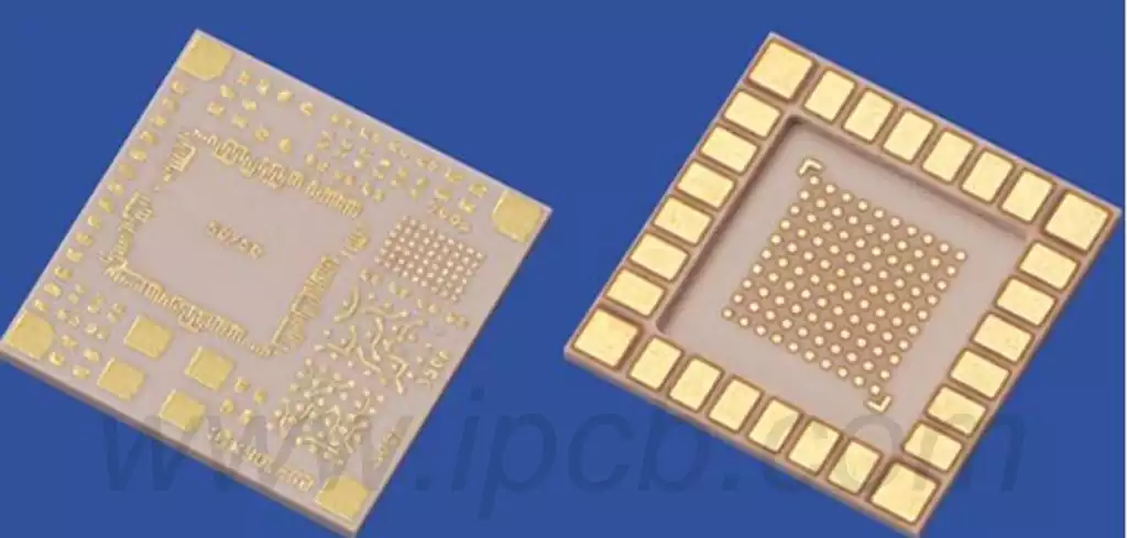
A ceramic pcb is a circuit board based on ceramic material, also known as a ceramic substrate or ceramic circuit board. It is prepared using ceramic powder and organic binder, and the circuit is prepared by printing conductive metal paste, which is sintered at high temperatures to form a pcb board. Ceramic printed circuit boards have the advantages of high heat resistance, high insulation, excellent thermal conductivity, miniaturization, and high reliability, so they are widely used in high-temperature environments, high voltage, and high current, high-speed digital signal processing, miniaturized devices, and high-reliability requirements.
Ceramic pcb board on the material requirements:
High-temperature stability:ceramic circuit boards need to be stable in high-temperature environments, so they must be made of high-temperature-resistant, non-deformable materials.At the same time, the coefficient of thermal expansion of the material to match the ceramic, to avoid deformation and cracking caused by temperature changes.
High insulation:Ceramic pcb is usually used in high-voltage,high-current application scenarios,so they need to have high insulation to ensure the safety and stability of the circuit.The material is required to have a high dielectric constant and low dielectric loss to ensure the signal transmission quality and energy efficiency of the circuit.
Excellent thermal conductivity:The thermal conductivity of ceramic circuit boards is essential to ensure the stability and reliability of the circuit. Requirements for materials with high thermal conductivity,can effectively transfer the heat generated by the circuit, and reduce the operating temperature of the circuit to prevent thermal failure.
Good processing performance:the manufacture of the ceramic board needs to go through complex processing, including cutting, grinding, polishing, etc..The material must be easy to process,with good plasticity and wear resistance to ensure processing quality and efficiency.
Chemical stability: ceramic circuit boards need to work in different environments, so the material is required to have stable chemical properties and be able to withstand a variety of environmental factors (such as temperature,humidity,atmosphere,etc.), to maintain the stability and reliability of performance.
Appropriate size and thickness:the size and thickness of the ceramic circuit board have an important impact on its performance and service life.The material is required to have the right size and thickness to meet the needs of the actual application.At the same time, the size and thickness of the material should be good stability to ensure no deviation in the manufacturing process.
Low cost: Ceramic circuit boards are more expensive,so low-cost materials are required to reduce overall manufacturing costs.
Ceramic pcb offers the following advantages over conventional FR4 pcb:
High heat resistance: Ceramic pcb material has a high melting point, so ceramic pcb has good heat resistance and can work stably in high-temperature environments.
High insulation: ceramic materials have excellent insulating properties, so ceramic printed circuit boards have high insulation resistance and dielectric loss, suitable for high-voltage, high-current application scenarios.
Excellent thermal conductivity: ceramic materials have better thermal conductivity, which is conducive to the heat dissipation of high-power electronic devices and improves the stability of the system.
Miniaturization: ceramic printed circuit boards can be made very thin and can be processed into a variety of complex shapes,which is conducive to the miniaturization of electronic equipment.
High reliability: the structure of the ceramic printed circuit board is stable,not easily affected by the environment, with high reliability and stability.
Compared with traditional PCBs, ceramic PCB has significant differences in environmental impact:
- Differences in energy consumption
Conventional PCB manufacturing processes usually involve significant energy consumption, especially in processes such as copper etching and glass fiber reinforcement. In contrast, the production of ceramic PCBs is also energy-intensive, but the materials used and structural properties allow them to perform well in high-temperature applications, with high thermal conductivity and the ability to operate at high currents with balanced heat dissipation. Therefore, although the production process of ceramic PCBs is also energy-consuming, but its later application potential will reduce the impact of energy consumption to a certain extent. - Recyclability
Conventional PCBs are composed of glass fibers and thermoset polymers, which usually cannot be recycled because their chemical bonding is irreversible . Ceramic PCBs are also relatively difficult to recycle today due to their complex material composition and high melting point. Although researchers are now developing recyclable PCB materials (e.g.,PCBs with “self-healing” polymers), the overall recyclability of ceramic PCBs is still limited. - Pollutant emissions and environmental regulations
Most of the chemicals involved in traditional PCB manufacturing contain substances that are harmful to the environment and the human body, such as lead and brominated flame retardants, which can lead to air and water pollution during production and use. Ceramic PCBs are able to reduce the emission of such hazardous substances during their use, especially in terms of their material selection in compliance with environmental regulations such as RoHS. However, the manufacturing of ceramic PCB still requires the use of energy-intensive chemical coating processes, which may put some pressure on the environment. - Sustainability Potential
In response to environmental concerns, the production of ceramic PCB is undergoing a number of sustainability measures, such as reducing environmental pollution by recycling copper and finding alternatives to less harmful chemicals. In addition, the inherent durability and better thermal management of ceramic materials give them the potential to reduce e-waste generation.
Ceramic circuit boards have a wide range of application scenarios, mainly including the following aspects:
Automotive electronics: automotive lights, automotive sensors, automotive power supplies,etc.
Medical equipment and instruments: artificial ear, medical cosmetology instruments,etc.
Semiconductor devices: heat-conducting sheet, cooling sheet, high-power module,etc.
Communication equipment: 5G base station, communication antenna substrate,etc.
Electronic devices: such as insulation resistors, resistance sensors,etc.
Industrial power supply.
Transportation rail.
High-power LEDs,etc.
As a high-performance circuit board material,ceramic pcb has many unique advantages and application prospects. Although there are some challenges in the application process, but with the continuous progress of technology and cost reduction, I believe that the application areas of this printed circuit board will be further expanded!