In the era of rapid advancement in artificial intelligence technology, AI servers are playing an increasingly pivotal role as the core infrastructure underpinning its operations. As the “nerve centre” of AI servers, the design and performance of PCBs (printed circuit boards) directly determine the overall efficiency and stability of the servers. However, AI server PCB design faces numerous unprecedented challenges while continually exploring innovative development directions.
Core Challenges in AI Server PCB Design
High-Speed Signal Integrity (SI) Challenges
Data traffic within AI systems is exceptionally voluminous. Take, for instance, the AI Memory PCB connecting GPUs to High Bandwidth Memory (HBM), and the AI Fabric PCB enabling high-speed interconnections between multiple accelerators. Signal rates have already reached 112 Gbps/s and are advancing towards 224 Gbps/s. At such extreme speeds, even minute signal distortion can trigger data errors. Temperature emerges as a critical factor affecting signal integrity, altering the PCB material’s dielectric constant (Dk) and loss factor (Df), which in turn impacts impedance and signal attenuation.
Power Integrity (PI) Challenges
AI chips impose exceptionally stringent power requirements, characterised by low voltages (typically below 1V), high currents (peaking above 1500A), and rapid transient responses (with currents fluctuating dramatically within nanoseconds). Any power noise or voltage sags may cause computational errors or even system crashes. Consequently, the Power Distribution Network (PDN) design within AI Server PCBs is paramount for ensuring power integrity. Supplying hundreds or even thousands of amperes of instantaneous current to AI chips within confined spaces while controlling voltage drops and noise presents an immense challenge.
Advanced Thermal Management Challenges
The latest AI chips from companies like NVIDIA, AMD, and Intel have easily surpassed 700W Thermal Design Power (TDP), advancing towards 1000W and beyond. Concentrating such immense energy within minuscule silicon wafers poses severe challenges for both thermal dissipation and power delivery across the entire system. When chip temperatures exceed thresholds, the system automatically activates protective mechanisms, reducing operating frequencies (known as ‘thermal throttling’), resulting in underutilised, costly AI computing power. Prolonged high-temperature operation also accelerates component ageing, shortens equipment lifespan, and increases operational maintenance costs. Moreover, high-speed signal transmission necessitates low-loss materials, yet these materials often exhibit poor thermal conductivity, creating a fundamental trade-off between high-speed performance and thermal management.
The Complexity-Reliability Paradox
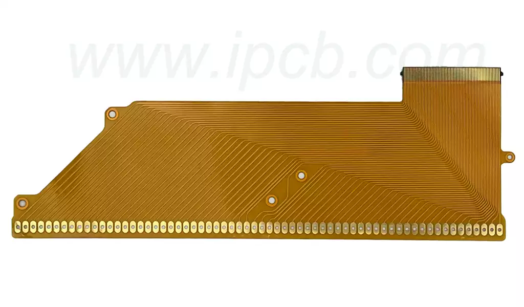
AI server PCBs typically feature 20–40 layers or more, alongside micron-level line precision and novel material applications. These factors impose exceptionally stringent demands on both manufacturing processes and long-term reliability.
Development Trends and Innovation Directions
High Layer Count Boards and High-Density Interconnect (HDI) Technology
AI servers impose far greater technical demands on PCBs than traditional servers, making high-layer count boards (HLC) and high-density interconnect boards (HDI) core requirements. For instance, high-speed PCBs with eight or more layers have become standard for AI servers. NVIDIA’s Rubin platform is projected to introduce an orthogonal backplane architecture by 2027, synthesising ultra-high-density 78-layer PCBs from three 26-layer boards. This will drive AI servers’ transition from copper cable interconnects to fully board-mounted interconnects. Complex routing demands for multilayer boards (e.g., 30+ layers) are particularly pronounced.
Advanced Material Selection
For signal integrity design, AI server PCBs employ ultra-low-loss materials. For instance, premium materials like Tachyon 100G and Megtron 7/8 maintain stable Dk/Df values across broad temperature ranges and high-frequency bands. As global server PCB production surges, future focus will centre on AI computing infrastructure development, where high-layer count boards (16+ layers) and ultra-low-loss materials (e.g., Megtron 6) will prove pivotal.
Precision Impedance Control and Optimised Routing Topology
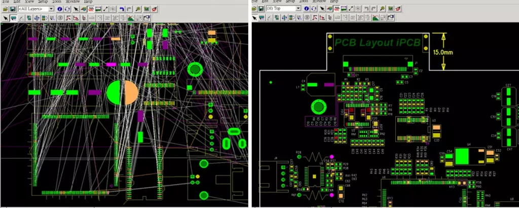
To ensure zero data distortion at elevated temperatures, AI server PCBs employ precise impedance control. Design and simulation are conducted based on material characteristics at target operating temperatures, maintaining differential impedance within stringent tolerances of ±7% or even ±5%. Optimised routing topologies are equally vital. Techniques like back-drilling eliminate signal reflections caused by via stubs, while controlling timing deviations through optimised trace length matching and minimised bends. Crosstalk suppression is achieved by adding stitching vias and guard traces between high-speed differential pairs, coupled with strategic stackup planning for effective shielding.
Thermal-Electrical Isolation Design and Embedded Cooling Technology
Confronted with kilowatt-level power consumption challenges, thermal-electrical isolation redesigns thermal pathways, making metal substrates and embedded cooling structures standard for high-power applications. The core value of AI server PCBs lies in advanced thermal management strategies, as external fans or liquid cooling plates alone cannot resolve chip-level hotspots. Heat must first be efficiently conducted from the chip to the PCB circuit board, then diffused through the PCB board to the heat dissipation module. Specific techniques include thick copper and ultra-thick copper processes (3oz to 10oz or even thicker copper foil), which significantly enhance lateral thermal conductivity. Thermal vias are arrayed beneath the chip to vertically conduct heat to the heat sink or internal thermal plane on the PCB’s reverse side. Embedded cooling technology (Embedded Coin) incorporates copper blocks or heat pipes directly within the PCB board, establishing direct contact with the chip’s underside to create highly efficient thermal pathways. High-thermal-conductivity substrate materials, such as Insulated Metal Substrates (IMS) or ceramic substrates, exhibit thermal conductivities tens or even hundreds of times greater than FR-4.
Application of AI Technology in Design Tools
The integration of artificial intelligence within PCB design tools is transforming PCB design workflows. Analysis of nine existing AI-driven PCB design tools, such as Flux.ai’s AI Copilot feature, demonstrates their formidable capabilities aimed at enhancing PCB design efficiency, precision, and user-friendliness. AI assists in optimising PCB layout, reducing signal interference, and improving routing efficiency.
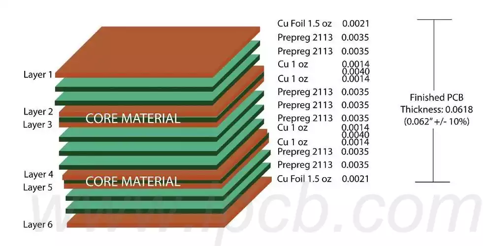
Complex Laminate Design
A typical AI server PCB features 20–40 layers or more. Planning layer functionality is crucial for balancing electrical performance, thermal management, and manufacturability. Laminate structures should maintain symmetry to prevent warping or buckling during thermal compression due to uneven thermal expansion. High-speed signal layers must adjoin complete ground or power planes to ensure clear return paths and precise impedance control. Establishing multiple pairs of power/ground planes not only reduces PDN impedance but also serves as shielding and aids thermal dissipation.
Amidst formidable challenges, AI server PCB design is advancing steadily through innovations such as high-layer count boards, HDI technology, advanced material selection, and precision impedance control. As these techniques continue to evolve and mature, AI server PCBs are poised to better meet the demands of artificial intelligence development, providing robust and reliable hardware foundations.