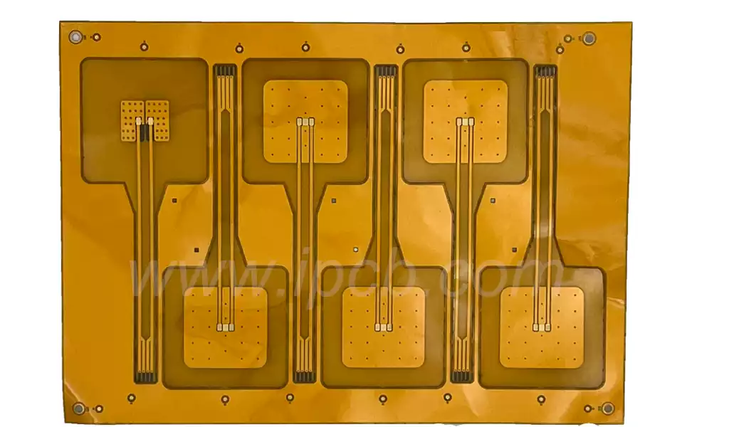
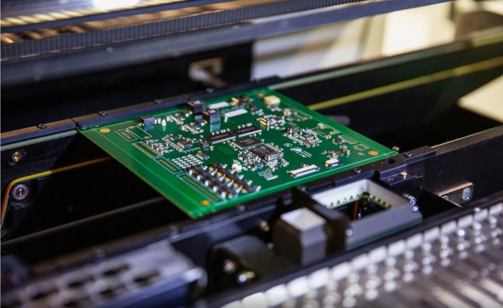
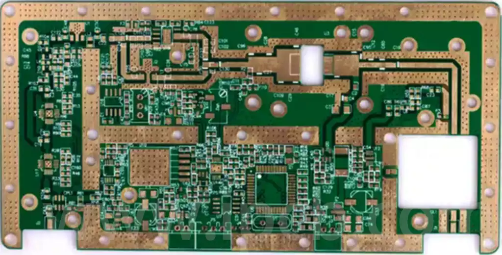
PCB layer stack, also known as PCB layering, is a common practice in electronic design, especially in devices that require high density and high speed signal processing. The central goal is to increase functionality and speed by stacking multiple circuit boards in the same device.
How does PCB layering work? In a nutshell, it accomplishes this by stacking multiple circuit boards on top of each other while ensuring that they have predefined interconnections between them. These multilayer PCBs usually consist of at least three conductive layers, with the bottom layer being synthesized with an insulating board.
The stacked design of PCBs is not a simple stacking of layers, where the arrangement of the ground layer is critical and is closely related to the arrangement and direction of the signals. Multilayer board design and ordinary PCB compared to the addition of the necessary signal alignment layer, the most important is the arrangement of an independent power supply and ground layer (laying copper layer). In high-speed digital circuit systems, the advantages of using the power and ground layer to replace the previous power and ground buses mainly lie in:
1) Providing a stable reference voltage for the conversion of digital signals.
2) Uniformly applying power to each logic device simultaneously.
3) Effectively suppress crosstalk between signals.
The reason is that the use of large-area copper as the power and ground layer greatly reduces the resistance of the power supply and ground, so that the power layer on the voltage uniformity and smoothness, but also to ensure that each signal line has a very close to the ground plane corresponds to, which at the same time also reduces the characteristic impedance of the signal line, but also can effectively reduce crosstalk. Therefore, for some high-end high-speed circuit design, it has been clearly stipulated that must use 6 layers (or more) of the laminated program, such as Intel’s requirements for PC133 memory module PCB. This is mainly to take into account the multilayer board in the electrical characteristics, as well as the suppression of electromagnetic radiation, and even in the resistance to physical and mechanical damage to the ability to significantly better than the number of low-layer PCB.
In general, are in accordance with the following principles of stackup design: to meet the signal characteristic impedance requirements; to meet the principle of minimizing the signal loop; to meet the requirements of minimizing the signal interference within the PCB; to meet the principle of symmetry.
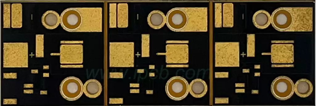
Specifically in the design of multilayer boards need to pay attention to the following aspects:
1) a signal layer should be adjacent to a copper layer, signal layer and copper layer should be placed at intervals, it is best that each signal layer and at least one copper layer adjacent.The signal layer should be tightly coupled to the adjacent copper layer (i.e., the dielectric thickness between the signal layer and the adjacent copper layer is very small).
2) The power and ground layers should be tightly coupled and in the middle of the stack. Shorten the distance between the power supply and the ground layer, which is conducive to the stability of the power supply and reduce EMI. try to avoid the signal layer sandwiched between the power supply layer and the ground layer.Power plane and ground plane close to each other is like the formation of a flat capacitance, when the two planes closer together, the capacitance value will be larger.The main function of this capacitance is to provide a low impedance return path for high frequency noise (such as switching noise, etc.) so that the power input to the receiver device has less ripple and enhances the performance of the receiver device itself.
3) in the case of high-speed, you can join the extra ground layer to isolate the signal layer, more than one layer of copper ground can effectively reduce the PCB impedance, reduce common mode EMI, but it is recommended that do not try to isolate the extra power layer, which may cause unnecessary noise interference.
4) high-speed signals in the system should be in the inner layer and between the two copper, so that the two copper can provide shielding for these high-speed signals, and the radiation of these signals is limited to two copper areas.
5) Priority is given to high-speed signals, clock signals, transmission line model, for these signals to design a complete reference plane, try to avoid the cross-plane split area, in order to control the characteristic impedance and to ensure that the signal return path is complete.
6) Two signal layers are adjacent to each other.For boards with high-speed signals, the ideal stack is to design a complete reference plane for each high-speed signal layer, but in practice we always need to make a trade-off between the number of PCB layers and PCB cost.In this case it is not possible to avoid having two signal layers next to each other.
The current practice is to let the two signal layer spacing and make the two layers of the alignment as vertical as possible, in order to avoid layer to layer signal crosstalk.
7) laying copper layer is best to set up in pairs, such as six-layer board 2, 5 or 3, 4 layers to lay copper together, which is considered a balanced structure on the process requirements, because the imbalance of the laying of copper layers may lead to PCB warping and deformation.
8) The sub-surface (i.e., the layer immediately below the surface) is designed as a ground layer, which is conducive to reducing EMI.
9) Estimate the number of required signal layers based on PCB device density and pin density to determine the total number of layers.
The structure of the board layer is to determine the EMC performance of the system is a very important factor. A good board layer structure to inhibit the PCB radiation plays a good effect. Most of the common high-speed circuit systems nowadays use multilayer boards instead of single and double-sided boards.
The main advantages of PCB layering include reduced impedance mismatch and signal crosstalk problems. However, it also presents some challenges. For example, without proper stacking design, electromagnetic emissions (EMI) may increase. Another common problem is layer offset, which can be prevented by designing the board side by side using heat fusing, riveting and pinning methods.
In the realm of electronic design, PCB layer stack is undoubtedly a delicate endeavor full of art and challenge. Through precise layer stacking design, engineers are able to create powerful and fast circuit boards that meet the high density and high performance demands of modern electronic devices. From the digital signal to provide a stable reference voltage, to uniform power supply, signal crosstalk suppression, and then to improve electromagnetic compatibility (EMC) and reduce electromagnetic radiation (EMI), multi-layer PCB stacking design in a number of ways to show its unique advantages.
