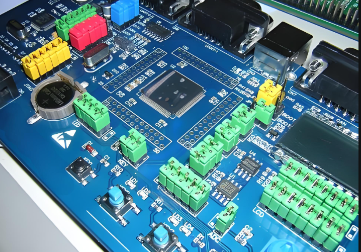
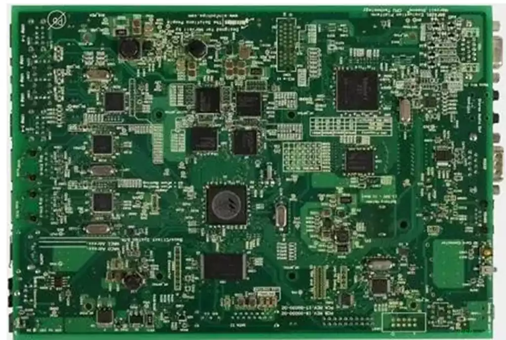
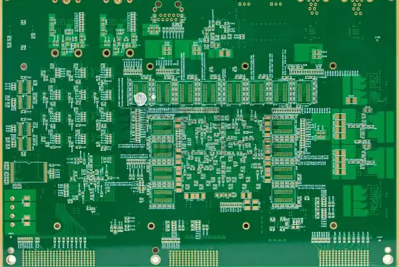
AI servers, as the pivotal infrastructure for computational power, face unprecedented challenges in their hardware design and manufacturing processes. High layer PCBs and flip-chip ball grid array (FC-BGA) carrier boards, serving as core components of AI servers, play a decisive role in system performance, reliability, and integration. However, the manufacturing of these two components involves complex material science, precision machining techniques, and process control challenges, becoming key factors constraining the performance enhancement of AI servers.
High layer PCBs: The Unsung Heroes of High-Speed Signal Transmission
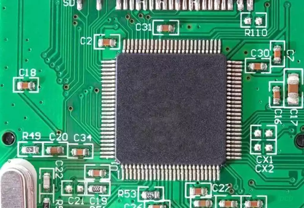
Within AI servers, high layer PCBs (typically referring to PCBs exceeding 20 layers) shoulder the critical responsibilities of high-speed signal transmission, high-power supply, and complex circuit integration. As AI chip computing power grows exponentially, PCB layer counts have surpassed 40 layers and beyond. Yet the tension between interlayer interconnect density and signal integrity has intensified—akin to managing high-speed traffic flow through narrow channels while ensuring each vehicle travels smoothly without collision.
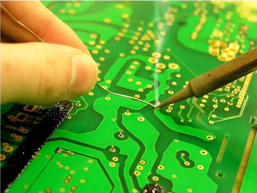
Through-hole processing: A dual challenge of materials and techniques
High layer pcbs frequently employ M6 and M7 grade high-frequency, high-speed substrates. These materials feature high glass fibre content and low dielectric constants, yet exhibit significantly increased hardness and brittleness. During through-hole drilling, micro-apertures below 0.2mm have become the predominant requirement. However, ultra-fine drill bits (e.g., 0.1mm diameter) suffer from poor heat dissipation and restricted chip evacuation pathways during machining. The intense friction between the drill and material resembles piercing hard rock with an extremely fine needle. This not only risks exceeding the critical threshold of 1.6μm for hole wall roughness (Ra value), potentially causing signal reflection and impedance mismatch that disrupts accurate signal transmission; Moreover, drilling multi-layered stacks of extremely thick boards (1.6–4.0mm) requires multiple drilling passes, with each pass processing several times the material volume of conventional PCBs. This is akin to a worker simultaneously drilling multiple heavy wooden planks, exponentially increasing workload and reducing drill needle lifespan by over 30%. Amidst fierce market competition and stringent cost controls, the tension between production capacity demands and cost management becomes particularly acute. Enterprises must maintain production efficiency while minimising costs – an undeniably formidable challenge.
High Drill Compensation and Stub Effects: A Difficult Balance to Achieve
To enhance signal transmission rates,back drilling technology is widely employed to eliminate residual copper stubs within vias. However, when drill depth compensation reaches D + 6 mil (approximately 0.15 mm), traditional CCD full-board compensation systems fail due to misalignment between mixed holes and via centres (typically ±25 μm). This is akin to aiming at a target where minor disturbances prevent precise hits. More critically, board thickness variations (e.g., ±5% lamination tolerance on 2.3mm substrates) cause stub lengths to fluctuate randomly between 2–8 mil. This uncertainty is akin to driving on an uneven motorway, where road undulations destabilise vehicle speed and handling, inducing phase noise in high-frequency signals. Particularly in SerDes channels exceeding 112Gbps, such phase noise can cause substantial bit error rate (BER) increases, severely compromising data integrity and posing potential risks to AI server stability.
Interlayer Alignment and Thermal Stress Management: The Balance Between Precision and Deformation
The interlayer alignment accuracy of high-layer-count printed circuit boards must be maintained within ±50μm. However, during high-temperature lamination, variations in the Coefficient of Thermal Expansion (CTE) between different materials can cause interlayer misalignment. For instance, copper foil (CTE ≈ 17 ppm/°C) and resin (CTE ≈ 50 ppm/°C) exhibit expansion discrepancies of up to 0.1% at lamination temperatures (180–200°C). For PCBs exceeding 40 layers, the cumulative effect of such minute expansion variations poses a direct threat to yield rates. This analogy mirrors constructing a skyscraper where minor deviations between each storey could cause the entire structure to tilt or even collapse. Consequently, the industry has adopted low-CTE resin systems and Laser Direct Imaging (LDI) technology. Material modification and precise exposure compensate for thermal deformation. Low-CTE resin systems function like a ‘snug, insulating coat’ for materials, minimising expansion and contraction due to temperature fluctuations. Laser Direct Imaging, meanwhile, acts as a meticulous artist, precisely etching required patterns onto substrates to enhance interlayer alignment accuracy.
FC-BGA Substrates: Pushing Micron-Level Precision to the Limit
FC-BGA substrates serve as the critical interface layer between AI chips and PCBs, primarily enabling high-density I/O interconnections and thermal management. As chip fabrication advances into the 3nm era, substrate routing density has surpassed 200 lines/mm², with line width/spacing (L/S) reduced below 8/8μm. This imposes exceptionally stringent demands on substrate manufacturing, akin to carving intricate patterns on the tip of a needle.
Resin Viscosity and Drilling Processes: A Conflicting Dilemma
FC-BGA substrates commonly employ BT resin or ABF materials with high glass transition temperatures (Tg > 200°C). While these materials’ low thermal expansion properties enhance chip packaging reliability, their high viscosity and toughness result in extremely poor chip removal efficiency during drilling operations. If debris within micro-holes (aperture < 0.1mm) is not promptly removed, it carbonises due to friction-induced heat, creating irreversible wall defects. This resembles debris clogging a narrow conduit, not only impeding fluid flow but also damaging the conduit itself. Consequently, drill bits require special coatings (such as diamond-like carbon films) to reduce friction coefficients, complemented by vacuum-assisted chip evacuation systems. The diamond-like carbon coating acts like a smooth outer layer on the drill needle, reducing friction with the material. The vacuum-assisted chip removal system functions like a powerful vacuum cleaner, promptly sucking away the chips generated during drilling. However, this increases the cost per hole by over 40%. While pursuing high-quality manufacturing, enterprises must also consider cost control.
Routing Density and Drilling Precision: A Challenging Trade-off in Manufacturing
Under routing density requirements, substrate drilling positional accuracy must achieve ±15μm (CPK ≥ 1.33), necessitating positioning system repeatability exceeding ±5μm. Traditional mechanical drilling machines, however, suffer from spindle thermal expansion, causing temperature drift of up to ±3μm/℃ during continuous operation. This is akin to a person experiencing slight tremors after prolonged work due to fatigue, leading to diminished machining precision. Consequently, such machines must operate within temperature controlled workshops (±0.5℃) to minimise thermal variations’ impact on accuracy. More problematically, with individual substrates now featuring over 500,000 holes and machining durations exceeding 20 hours, taper accumulation from drill bit wear can reach ±8μm. This parallels a knife becoming dull over prolonged use, where cutting dimensions gradually lose precision. To resolve this, a dynamic compensation algorithm must adjust feed rates in real time. This functions like equipping the machine with an intelligent ‘brain’ that automatically modifies processing parameters based on drill bit wear, thereby safeguarding machining precision.
Microvia Metallisation and Signal Loss: A Difficult Trade-off
To achieve low-loss transmission of high-frequency signals, the uniformity of copper plating within carrier board microvias must be controlled within ±3μm. However, when aperture sizes shrink to 0.05mm, the fluidity of the plating solution decreases, exacerbating uneven copper thickness distribution within the holes. While pulse plating and additive optimisation can improve deep plating capability, they introduce organic impurities, causing dielectric loss (Df value) to rise above 0.005. This situation is akin to applying conductive material to a delicate circuit board, where uniform coating must be ensured without introducing impurities that compromise circuit performance. This contradiction becomes particularly acute in the 112GHz millimetre-wave band, as even minute signal losses at high frequencies can degrade signal quality. Therefore, overcoming this bottleneck requires synergistic innovation in both materials (such as modified polyimide) and processes (such as ALD atomic layer deposition). Modified polyimide materials offer superior electrical properties and thermal stability, while ALD technology enables precise control over coating thickness and quality, providing novel solutions to this challenge.
Small Module PCBs: Emerging Demand for High-Precision Forming
The modular design of AI servers has driven explosive growth in demand for miniaturised PCBs, including optical modules and HBM memory modules. During forming processes for such boards, hole-to-edge alignment precision of ±35μm is required, rendering the ±80μm tolerance achievable by conventional mechanical forming machines inadequate. Much like crafting a minute component where extreme precision is essential to ensure performance and quality, traditional methods now fall short. CCD optical forming machines employ high-resolution cameras (5μm pixel pitch) to capture positioning markers in real time. Combined with motion control algorithms that dynamically compensate tool paths, they elevate precision to ±15μm. The high-resolution camera functions like a pair of keen eyes, capturing every detail with accuracy; the motion control algorithm acts as a flexible brain, adjusting tool paths in real time based on captured data. However, this technology demands exceptionally stringent requirements for vibration suppression, light source stability, and algorithmic latency (necessitating <1ms), resulting in equipment costs 3–5 times higher than conventional solutions. This parallels the necessity of employing more advanced equipment and complex technologies to manufacture high-precision instruments, alongside incurring significantly greater expenditure.
AI server PCB manufacturing confronts multifaceted challenges across multiple domains, from high layer pcbs and FC-BGA carrier boards to small-module PCBs, with complex issues intertwining at every stage. Nevertheless, the industry is actively addressing these hurdles through material innovation, process refinement, and the introduction of new technologies, striving to overcome bottlenecks and explore viable pathways for enhancing AI server performance and ensuring stable operation.