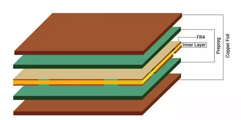
The production process for high-frequency microwave pcb is complex and requires extremely high precision, encompassing multiple critical stages from engineering data processing to final forming. To ensure product quality and performance, manufacturers must strictly adhere to specific operational procedures and control points at every stage of the process.
Challenges in high-frequency microwave pcb processing:
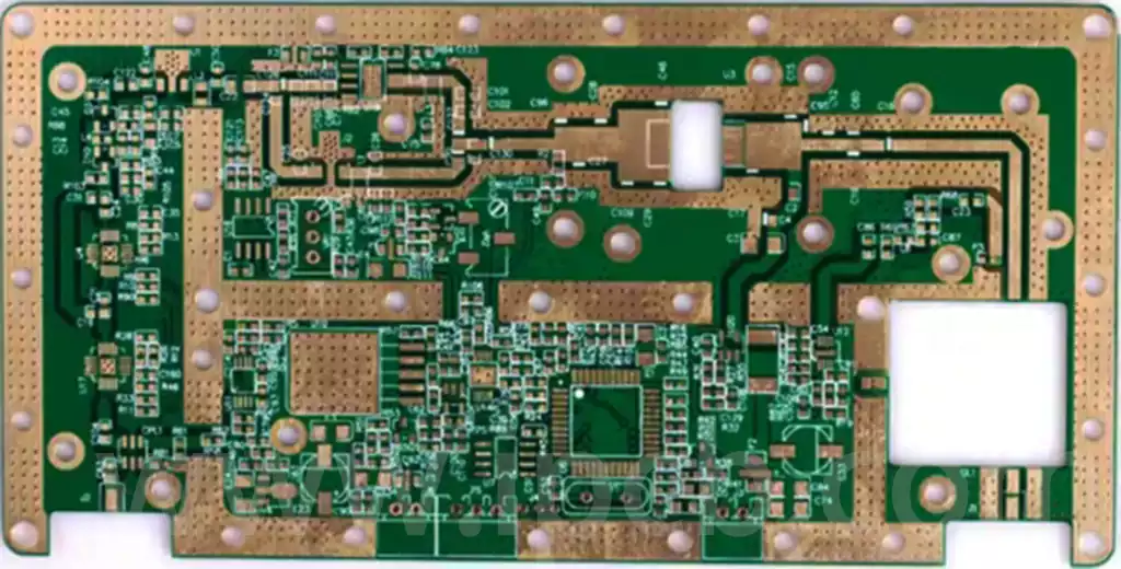
- Drilling: The substrate is soft, so the number of layers in the drilling stack should be minimised; typically, two layers are recommended for 0.8mm thick boards. The spindle speed should be slower, and new drill bits must be used, with specific requirements for the drill bit’s top angle and thread angle.
- Solder mask printing: After etching high-frequency microwave pcb/Rogers high-frequency pcb boards, the substrate must not be polished with a roller brush before applying the solder mask green oil to avoid damaging the substrate. Chemical surface treatment is recommended. Achieving this—no polishing, uniform and consistent circuit patterns and copper surfaces after solder mask printing, with no oxide layer—is no easy task.
- Hot air leveling: Due to the inherent properties of fluororesin, rapid heating of the board should be avoided. A preheating treatment at 150°C for approximately 30 minutes should be performed before tin plating, followed by immediate tin plating. The tin bath temperature should not exceed 245°C, as this may affect the adhesion of isolated pads.
- Milling the outer shape: Fluororesin is soft, and ordinary milling cutters produce excessive burrs and uneven surfaces when milling the outer shape. Specialised milling cutters must be used for this process.
- Inter-process transportation: The pcb boards must not be stored vertically; they must be placed flat in trays with paper between them. Throughout the process, the circuit patterns on the boards must not be touched by fingers. Throughout the process, prevent scratches, abrasions, line scratches, pinholes, indentations, and dents, as these can affect signal transmission. High-frequency microwave pcb/Rogers high-frequency pcb boards will be rejected.
- Etching: Strictly control side etching, serrations, and notches. Line width tolerance must be strictly controlled within ±0.02 mm. Inspect using a 100x magnifying glass.
Key Considerations in the Production of High-Frequency Microwave PCB
Engineering Data Processing
When performing CAM processing on customer files, manufacturers must fully understand the precision requirements for transmission line fabrication. Additionally, they must consider their own manufacturing capabilities and apply appropriate process compensation to ensure alignment between design and production. The production of high-frequency microwave pcb begins with precise processing of engineering data, which is critical for ensuring the accuracy of transmission line fabrication.
Material Cutting
Unlike conventional pcb boards, the material cutting methods for high-frequency microwave dielectric materials must be selected based on their distinct dielectric properties. Milling is typically the primary method to avoid compromising material flatness and board surface quality. For example, after cutting PTFE (polytetrafluoroethylene) sheets, if there are excessive burrs, 2000-grit sandpaper must be used for grinding, while taking care to prevent scratches. In special cases, a router may be used for cutting.
Drilling
For different dielectric materials, drilling parameters vary, and there are specific requirements for the drill bit’s point angle, flute length, and helix angle. For aluminium-based or copper-based microwave dielectric materials, drilling methods also differ to prevent burr formation. For example, the UC drill bit (Undercut Drill) reduces contact area during drilling to achieve high-quality hole walls, commonly used for processing special materials such as lead-free, halogen-free, high-Tg, and PTFE. When drilling, use a new drill bit, maintain a slow feed rate, preferably drill single holes, and ensure no water enters the hole.
Via Grounding
Via grounding typically employs chemical copper plating. During chemical copper plating, either chemical or plasma methods can be used; from a safety perspective, the plasma method is more effective. For aluminium-based microwave dielectric materials, conventional chemical copper plating is challenging. It is recommended to use metal conductive materials for via grounding, with the via resistance typically less than 20 mΩ. Plasma treatment (PLSMA) is a special processing method that uses a plasma device to treat internal adhesive residues in PTFE materials, but it is costly, and copper plating must be performed within 4 hours after processing.
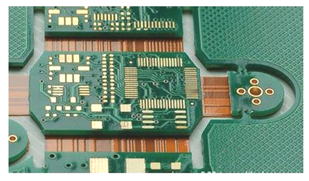
Pattern transfer
Pattern transfer is a critical process for ensuring pattern accuracy. When selecting photosensitive materials such as photoresist, wet film, or dry film, they must meet the requirements for pattern accuracy. Additionally, the light source of the photolithography machine or exposure machine must meet the process requirements. In circuit production, inner layer circuits use fully automatic wet film coating machines, while outer layer circuits use fully automatic film application machines. Both inner and outer layer circuit exposures are performed using fully automatic exposure machines and development + vacuum acid etching machines, with exposure energy controlled at 7–9 units and development at 40–60%. This method effectively controls line width tolerance within ±0.02 mm, ensuring the stability of the product’s signal.
Etching
The etching process must strictly control process parameters such as the concentration of etching solution components, temperature, and etching speed. During etching, burr control must be prioritised. Typically, line width requirements are ±20μm, and mass etching can only proceed after the first board is confirmed to have no burrs or gaps and meets line width standards. The goal is to ensure that the edges of the conductors are neat, free of burrs or gaps, and that conductor precision remains within tolerance requirements. Vacuum etching machines ensure uniformity of the circuit patterns across the entire workboard after etching.
Plating
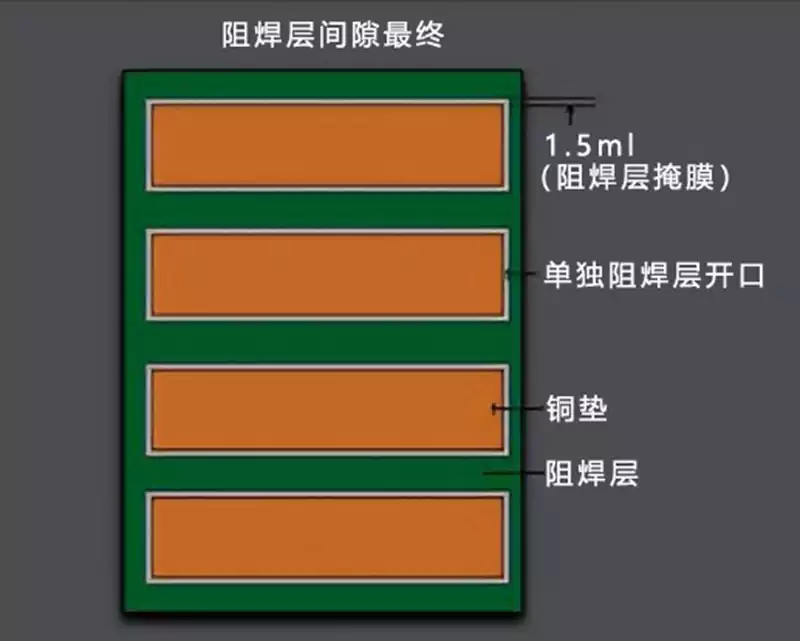
The final coating on the conductors of high-frequency microwave pcb typically includes tin-lead alloys, tin-indium alloys, tin-strontium alloys, silver, and gold, with pure gold plating being the most common. The thickness and uniformity of the plating layer must be strictly controlled. The characteristic impedance is related to the thickness of the copper foil, and for microwave boards with metallised holes, the plating thickness is particularly critical. After gold plating, a green solder resist peel test must be conducted to ensure no solder resist peeling occurs when pulling the 3M tape at a 90-degree angle before mass production.
Forming
The forming of high-frequency microwave pcb primarily uses CNC milling, but milling methods vary significantly depending on the material. Milling of metal-based microwave boards requires neutral coolant for cooling, and milling parameters differ greatly. During forming, the workbench must be kept clean. The layering method involves placing a used FR-4 bare board or phenolic board first, followed by the PTFE board to be formed, then another FR-4 bare board or phenolic board, and finally feeding the routing tape to prepare for routing. When milling the board, a return milling method is typically used to reduce burrs. The milling cutter should be replaced with a new one every 20 feet, and the milling speed should not be too fast. When removing the board after milling, special care must be taken, as the PTFE material is relatively soft and the holes are prone to deformation. Force should not be applied when removing the board. In special cases, an automatic de-pinning milling machine can be used to ensure precision and reduce hole breakage abnormalities.