As a key necessary step in the integrated circuit manufacturing process, chip packaging and testing plays a vital role. Specifically, this link will carry out a series of fine operations on the wafers that have passed the quality inspection, and complete the wafer cutting, chip welding and overall plastic sealing processes with the help of high-precision technology. Its core objective is to ensure that the chip’s internal precision circuitry and external devices to establish a stable and efficient electrical connection between the channel. In addition, package testing can also build a solid mechanical and physical protection barrier for the chip, effectively avoiding the risk of scratches and breakage that may easily occur due to the tiny and thin characteristics of the chip itself.
Encapsulation has placed, fixed, sealed, protect the chip and enhance the role of electrical and thermal properties, but also to communicate the internal world of the chip and the external circuit of the bridge – the chip on the contacts with wires connected to the sealing shell of the pins, these pins and through the printed circuit board on the wires and other devices to establish a connection. Therefore, package testing plays a vital role in the field of integrated circuits.
Detailed flow of chip packaging testing:
Wafer Testing
In the IC manufacturing process, wafers undergo a rigorous testing process to fully verify the functionality of the die before they enter further processing. During the testing process, the die are accurately categorised into three types: Good Die, which are fully functional with acceptable performance; Defective Die, which have localised imperfections or defects; and Failed Die, which are completely non-functional and unable to function properly. Defective Die’ with partial flaws or defects; and “Fail Die” with complete failure and no normal operation. According to the strict quality standards and classification criteria for product shipment, only those dies that meet the established requirements will be selected for the next stage of packaging production. This critical test process, known in the industry as chip packaging test, is known as Chip Probing Test (wafer probe test). The test principle is to establish an electrical connection with the pads on the surface of the die with the help of a precision probe, so as to conduct a comprehensive inspection of the function of the die to ensure that its performance is normal and in line with the design requirements.The importance of chip packaging test as an important line of defence to ensure the final quality of the chip is self-evident.
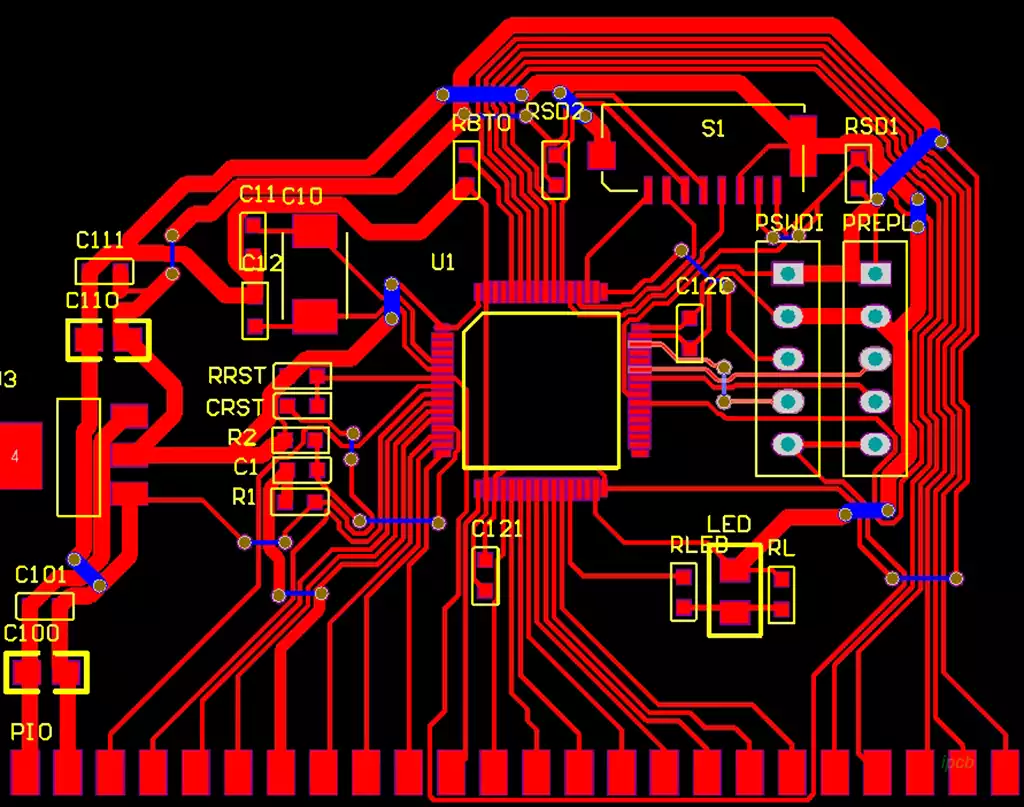
The core execution of chip packaging test relies on a set of sophisticated equipment and test component system, mainly including ATE test machine (Automatic Testing Equipment, i.e., automated test equipment, is responsible for providing stable power supply, precise signals, and specific function vectors for the chip test, and at the same time, real-time acquisition of the chip’s output feedback signals, and analysing and judging the test results through algorithms), Prober, a high-precision mechanical platform used to accurately carry wafers and achieve micron-level displacement to ensure that the probes on the probe card can be accurately aligned with the pad pins of the die and form a reliable electrical conduction), as well as customised test probe cards (Probe Card, which is tailored according to the unique circuit architecture and test requirements of each chip and undertakes the role of ATE). (a component tailored to each chip’s unique circuit architecture and test requirements that serves as a bridge between the ATE test channel and the chip’s Pad pins). These three types of core equipment and components work closely together to fully test and verify each die on the wafer, one by one. Once found abnormal function of the die, usually using ‘Ink Dot Marking’ and other visual marking means, in its surface for clear identification, in order to quickly and accurately complete the subsequent packaging production process of defective products rejected and screening of good products.
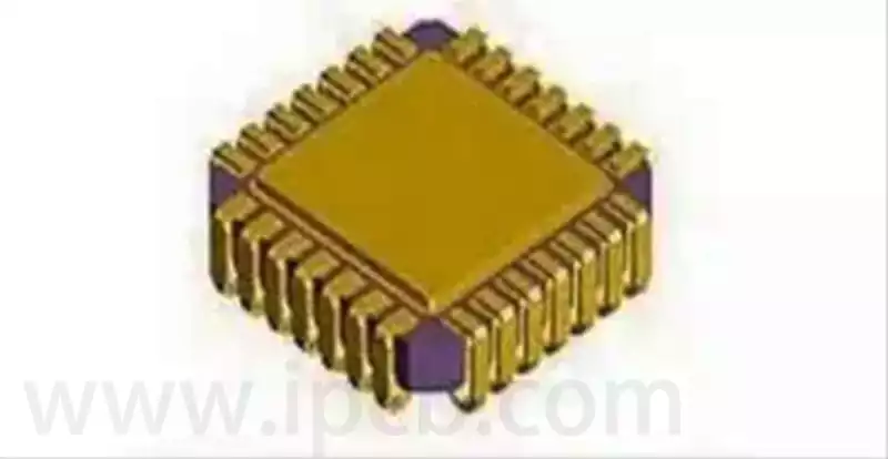
Chip Packaging (Assembly)
In the integrated circuit manufacturing process, after the wafer completes chip packaging test (wafer probe test), only the die with normal function and passed the test verification will enter the subsequent packaging production process. This pre-testing mechanism can accurately eliminate defective wafers, avoiding the waste of raw materials, manpower and equipment resources brought about by ineffective packaging, and effectively controlling manufacturing costs. Although there is a special process path of ‘blind packaging’ – that is, skipping the chip packaging test directly on the whole wafer packaging, followed by quality screening through the into the test link, but the application of the programme has significant limitations. Its core value is reflected in the early stage of chip development and engineering verification phase, such as after the flow of the chip need to quickly obtain engineering samples to verify the feasibility of the design, process maturity and basic functionality, blind sealing strategy can shorten the project cycle. However, when the product enters the mass production stage, the defect screening function of chip packaging test becomes a key technology node to guarantee the yield and control the cost, and it is an indispensable quality control means in the large-scale production.
Chip packaging process presents significant technical differences due to the diversity of its terminal form. Take the mainstream wire bonded ball grid array package (WB-BGA) as an example, its process completely covers the core technology of modern chip packaging.
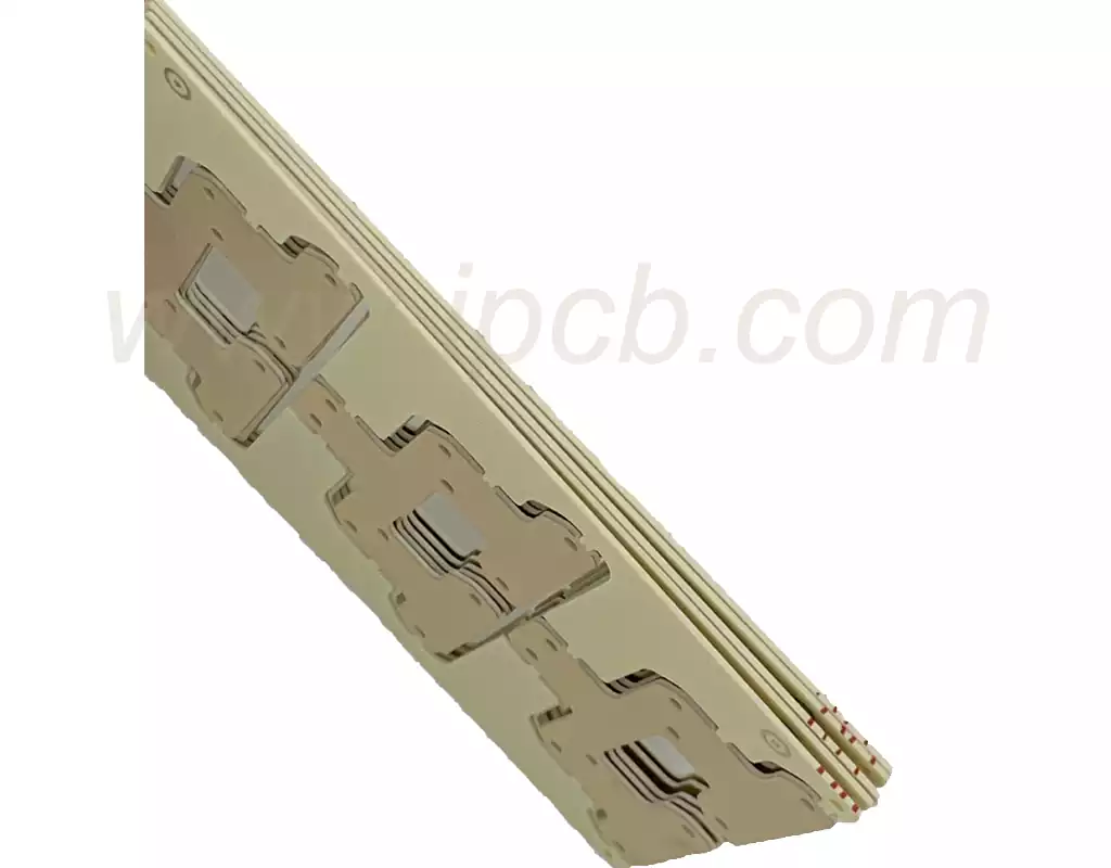
Wafer dicing, as the core technology of the pre-packaging process, requires precise deconstruction of wafers that have completed chip packaging testing into individual die units. The process requires the implementation of multi-dimensional process control: first of all, the wafer surface quality review, to confirm that there are no cracks, scratches and other structural defects; then attached to the front of the wafer high-strength UV adhesion reduction film or blue film, through the vacuum adsorption technology to eliminate the cutting vibration impact on the grain; for high-power chips or ultra-thin packaging needs, the need to use the chemical-mechanical polishing (CMP) and mechanical grinding composite process to reduce the wafer thickness from 700-800μm step-by-step. For high-power chips or ultra-thin package requirements, chemical mechanical polishing (CMP) and mechanical grinding composite process should be adopted to gradually reduce the wafer thickness from 700-800μm to 50-200μm, and at the same time, ensure that the wafer global thickness tolerance is controlled within ±3μm; the cutting link selects the process route based on the material characteristics of the wafer, and the composite solution of laser invisible cutting + diamond blade finishing is commonly adopted for silicon-based wafers, and the laser parameter is accurately controlled in the range of 1064nm wavelength, pulse width <50ns, and the blade speed is 30,000nm. The blade speed of 30,000-60,000rpm precision processing, to ensure that the cutting channel width error <± 2μm. the process of equipment precision requirements are stringent, the world’s leading companies such as Japan’s DISCO’s DAD3240 series of scribing machine through the two-axis linkage system to achieve a 0.1μm level of positioning accuracy, ACCRETECH’s DFG8560 is used in AI vision compensation technology to improve the quality of cutting; domestic manufacturers JXSON’s DFG8560 is used to improve the quality of cutting; domestic manufacturers JXSON’s DFG8560 is used to enhance the quality of cutting. Enhance the cutting quality; domestic manufacturers Jingsheng E&M’s JSSD-8200 and the WSD-8000 scribing machine of the 45th Institute of CEC, through the self-developed multi-axis linkage algorithms and dynamic pressure control system, have reached ±1.5μm processing accuracy in the field of 12-inch wafer cutting, marking the technological breakthrough of domestic equipment in the field of high-end packaging.
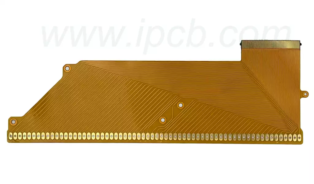
As the core carrier of electrical interconnection between the chip and the external system, the package substrate (SUB) is essentially a highly customised high-density interconnection (HDI) printed circuit board. Its design needs to take into account the chip Pad distribution density (usually up to 50-1000 I/O/mm²), signal transmission rate (up to 32Gbps), the coefficient of thermal expansion to match (CTE <7ppm / ℃) and other key parameters, through the buried micro-via (μVia), the ladder copper pillars (Copper Pillar), and other advanced structures to achieve the Pad to Ball Electrical extension. Take FC-BGA package substrate as an example, the number of line layers can reach 12-16 layers, line width/line spacing exceeds 1μm/1μm limit, the use of ABF (Ajinomoto Build-up Film) material to construct the layer structure can achieve 8-10μm fine line forming.SUB manufacturing needs to be integrated with advanced processes such as semi-additive process (SAP), modified semi-additive process (mSAP), etc., together with laser direct manufacturing. The manufacturing of SUB requires the integration of semi-additive process (SAP), modified semi-additive process (mSAP) and other advanced processes, together with laser direct imaging (LDI) and plasma etching technology, to ensure that the impedance control accuracy of ±5%, the degree of inter-layer alignment of <± 3 μm. The performance of this component directly determines the electrical performance of the chip, heat dissipation efficiency and long-term reliability, and it is the core breakthrough point of the iteration of packaging technology.
Chip packaging and testing as the IC industry towards the terminal application of the key ‘foot in the door’, its technological evolution has always been with the chip miniaturisation, high performance and functional integration trends resonate with the same frequency. With the rise of advanced packaging technologies such as 2.5D/3D stacking and Chiplet heterogeneous integration, packaging and testing is leaping from the traditional ‘back-end process’ to a key technology hub that determines chip performance, power consumption and cost.