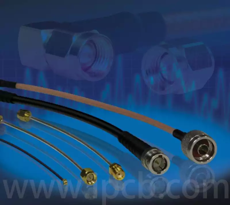
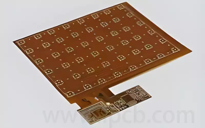
Circuit board side plating, also known as edge copper plating, refers to copper plating applied to at least one of the side edges of a PCB board that extends from the top to the bottom of the board. This process is designed to enhance the robustness of the PCB connection and reduce the risk of device failure, and is particularly important on small PCBs and motherboards, where this type of plating technology is particularly common in components such as Wi-Fi and Bluetooth modules. In the production process, the edges to be metallised are milled before the copper plating step. After the copper is deposited, the edges of the PCB undergo the necessary surface treatment.
When to use circuit board side plating, i.e. in which specific situations will edge plating be implemented:
When there is a need to enhance the conductive connection at the edge of the PCB: If the design of the PCB requires an efficient conductive connection at the edge section, then side plating is an effective solution.
When the edges of the PCB need to be used as conductive interfaces: If the edges of the circuit board are set up as critical parts for electrical connections to other components or circuit boards, then edge copper plating is necessary.
When the printed wiring board needs to improve its resistance to lateral impacts: Side plating can provide additional protection to the edges of the PCB, thus improving its ability to resist external lateral impacts.
When a secondary circuit board needs to be connected to the motherboard through its edges: In some designs,a secondary PCB may be connected to the motherboard through its edges, and copper plating on the edges ensures the reliability and stability of the connection.
For improved assembly and the need for PCB edge soldering: If the edge of the circuit board needs to be fixed or connected to other components through soldering, then side plating can provide a good soldering surface, thus improving the assembly process.
Types of circuit board side edge plating:
1.Full wrap-around edge copper plating
This process routes the circuitry along the metal edges of the holes after they are drilled. This wiring process brings the sidewalls of the PCB into contact with the chemically plated base copper, ensuring that the holes are processed for drilling and plated at the same time. Here is an example: first, a conductive surface is created on the base layer, which is then plated with a thicker, more durable copper layer for better adhesion.
2.Edge of copper plate
In order to avoid damage to the copper material, we usually set a minimum safe distance between the copper features (e.g. copper wiring or copper plating) and the edge of the PCB. The specific requirements of these distances are as follows: on the outer layer, the distance should not be less than 0.25 mm; if the inner layer with a breakout, the distance needs to be expanded to 0.40 mm; for all layers with a breakout, the distance should be up to 0.45 mm; and if the edge of the V-shaped cut marks, the same should follow the principle of the minimum distance of 0.45 mm.
The distance between the copper and the edge of the board applies mainly to flat areas and large areas of copper plating, where minor damage to the copper layer does not significantly affect the performance of the board. To ensure that the board is not damaged, wires (or traces) should be avoided being set within these specified minimum distances. If a pad inadvertently falls within this minimum distance boundary, trimming measures will normally be taken to ensure that the minimum copper-free area required is restored, except in the following cases:
Where the pads are part of an edge connector (such connectors often come with a bevelled design to suit the installation), they may be exempt from this restriction.
The same distance rule does not apply if the pad is specifically labelled in the mechanical layer as ‘extendable to board edge’.
If the trimming operation will result in a reduction of the pad surface area by more than 25%, this is usually considered an anomaly and may require design reconsideration or other solutions.
3.Plate Through Hole (PTH)
Plate Through Hole (Plate Through Hole) refers to the plated through holes opened at the edge of the board, these holes are also known as butterfly holes, their main purpose is to achieve the connection between the two PCBs through direct soldering or the use of connectors. In order to ensure that the boards are securely fixed to the production panel during the manufacturing process, the edges of the PCBs must be left free. At the same time, pads need to be placed on both the top and bottom layers of the board to ensure that the plating is securely anchored to the board. When it comes to smaller application scenarios, a gold finish is often considered preferable.
Sufficient unoccupied space must be left at the edges of the circuit board in order to securely anchor the circuit board to the production panel during the manufacturing process. At the same time, pads need to be arranged on the top, bottom (and possibly inner) layers to ensure that the plating layer is tightly and securely attached to the circuit board. As a general principle, the size of the holes should be enlarged as much as possible in order to enable better soldering with the parent PCB, with 0.80 mm or more being the recommended choice. As for the surface treatment, although a variety of treatments can be used, but in the face of smaller applications, I personally prefer to choose the gold treatment rather than nickel treatment.
4.Round Edge Plating
Rounded edge plating refers to most or even all of the circuit board or its cutout area, from the top to the bottom of the implementation of the plating process. The main purpose of this process is to provide a quality ground connection to the metal case or shield.In order to manufacture such boards with rounded edge plating, the contour of the pcb board is usually milled prior to the through-hole plating process.However,as the board needs to be held within the production panel during the plating process,it is not practical to achieve 100% edge plating.The limitations imposed by this must be taken into account when laying out the routing tabs.For round edge plating,the use of a chemically nickel-gold finish is seen as an ideal option.
Caution:
Each edge needs to be equipped with a copper strip to ensure that the plated connection is realised. However, full 100% plating coverage of the edges cannot be achieved as the board needs to be secured within the production panel during processing. Mechanical layers requiring rounded edge plating should be clearly labelled in the relevant drawings. For rounded edge plating, selective electroless nickel-gold surface treatment is considered the only applicable method.
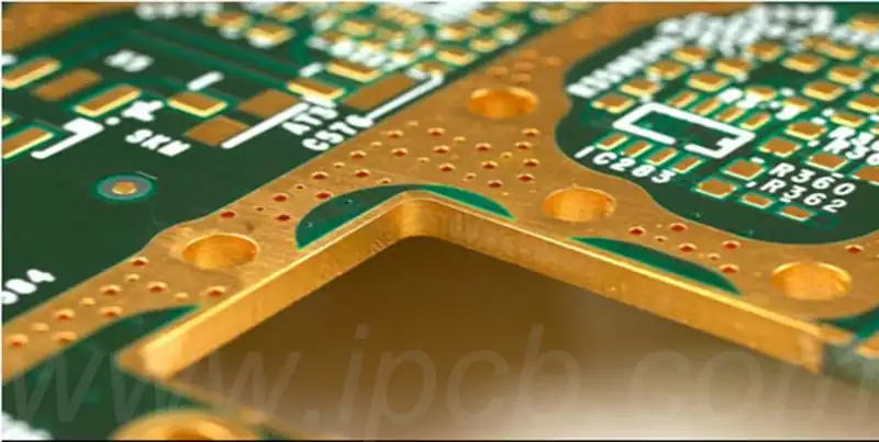
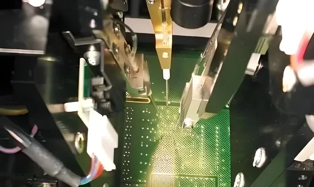
Circuit board Edge Plating Process
Precision drilling: It all starts with precision, with holes delicately drilled along the edge of the circuit board to reserve a place for the edge contacts or connectors to be installed.
Double Copper Plating: The PCB embarks on a double journey of copper plating. First, in the chemical copper plating bath, a uniform layer of fine copper is deposited evenly across the PCB and extends to the edges, providing a conductive base for subsequent plating operations. Immediately afterwards, the PCB enters the electrolytic copper plating process, where the edges are carefully plated with a thicker layer of copper to ensure excellent conductivity and durability.
Fine Etching: After plating is complete, the circuit board undergoes an etching process designed to remove excess copper material and precisely outline the desired line pattern. This critical step determines the precise shape and layout of the edge contacts.
Surface prep: The edges of the circuit board undergo a series of meticulous surface prep steps, including micro-etching. This orderly preparation removes any surface oxides or contaminants, which enhances the adhesion of the plating and ensures full plating coverage.
Dip Plating: Pre-treated edges are dipped into a plating solution containing precious metals such as gold or other metals known for their excellent electrical conductivity and corrosion resistance. The dip plating process deposits a fine layer of the selected metal on the bare copper surface, including the edge.
Cleaning and Drying: After plating, the circuit board undergoes a rigorous cleaning process to completely remove any residues or contaminants. This rigorous cleaning step ensures the integrity of the plated edges. The boards then undergo a thorough drying process to prepare them for the subsequent manufacturing process.
Quality Inspection: The finished edge-plated PCB is subjected to an exhaustive quality inspection. This comprehensive assessment covers the thickness of the plating, the uninterrupted continuity of the edge contacts and the identification of any anomalies or defects. This rigorous review ensures that the edge plating is in full compliance with established specifications and stringent quality standards.
Electrical Testing (if applicable): Depending on the specific needs of the PCB and the application scenario, an optional electrical testing phase may be performed. This test is designed to verify the functionality and performance of the edge contacts, as well as the overall electrical connection, to ensure that there are no uncertainties.
Circuit board side plating technology significantly enhances the connection robustness and electrical performance of PCBs through its sophisticated process steps and diverse application types. This technology not only improves the reliability and durability of electronic products, but also provides solid technical support for the trend of miniaturisation and integration of modern electronic equipment.
With the continuous progress of technology, circuit board side plating technology will continue to play a key role in the electronics manufacturing industry.