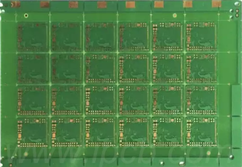
IC board, i.e. packaging substrate, is a kind of circuit board used to carry chips, belongs to a branch of PCB, has the characteristics of high density, high precision, high performance, miniaturisation and thinness, which can provide support, heat dissipation and protection for the chip, and also provide electrical connection and physical support between the chip and the PCB motherboard.
IC board is the key component of chip packaging, which is the carrier for connecting and transmitting signals between the bare chip (DIE) and the printed circuit board (PCB).
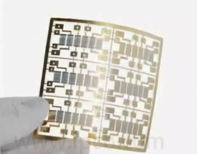
Compared with ordinary PCB products, its product size is smaller and more precise, and it requires very high requirements in terms of line fineness, hole spacing size and signal interference, so it needs highly precise interlayer alignment technology, plating capability and drilling technology.
Classification of IC board:
Classification by package: It can be divided into four categories: WB (Wire Bonding), FC (Flip Chip), BGA (Ball Grid Array) and CSP (Chip Scale Package), of which FCBGA (Flip Chip Ball Grid Array) has the highest technical requirements.
(1) WB/FC is the main connection between the bare chip and the carrier board.
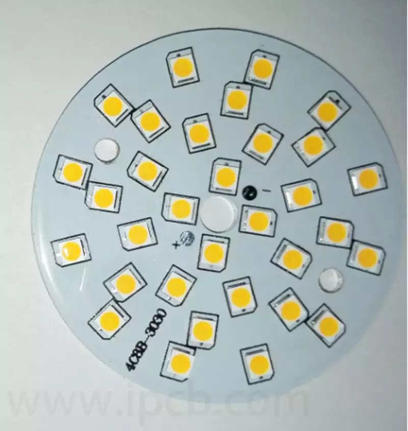
WB (Wire Bonding): through the metal lead to the bare chip and the carrier board connection. WB process using fine metal wires, the use of heat, pressure or ultrasonic energy to make the metal lead and chip pads and substrate pads closely welded to achieve electrical interconnections between the chip and the substrate as well as between the chip and the transmission of information. The technology is widely used in the packaging of RF modules, memory chips and microelectromechanical systems (MEMS) devices. For example, RF modules are mainly used for wireless RF power amplifiers, transceivers and front-end receiver modules; digital modules are commonly used in digital camera memory cards and other devices.
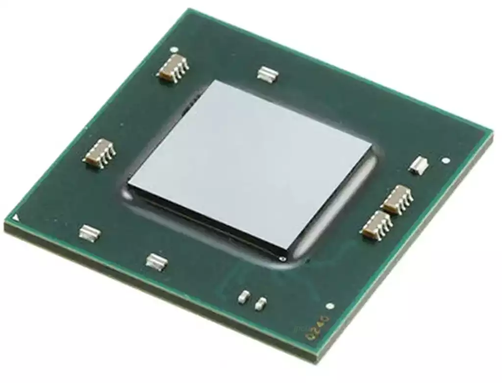
FC (Flip Chip): The bare chip is flipped on its front side and connected directly to the carrier board through solder ball bumps, which serve as a buffer medium for the electrical connection and signal transmission between the chip and the board.FC technology uses solder balls to connect the chip to the substrate, flips the chip and attaches it to the corresponding substrate, and heats up and melts the solder balls to achieve the bonding of the chip to the substrate pads. Compared with WB, FC uses solder balls instead of leads, which significantly improves the signal density and chip performance of the carrier board, while bump alignment correction is more convenient and improves the production yield, making it a more advanced connection method. At present, FC technology has been widely used in CPU, GPU and other high-performance chip packaging.
(2) BGA/CSP is the main connection between carrier board and PCB.
BGA (Ball Grid Array, Ball Grid Array Package): multiple tin balls are arranged in an array at the bottom of the chip, and the tin ball array is used to replace the traditional metal wire frame as a pin.BGA is a high-density packaging technology, unlike other packaging methods, its pins are distributed at the bottom of the package, which makes the pitch of the I/O terminals increase, and is able to accommodate a larger number of I/O.BGA package is a high density packaging technology, which is different from other packaging methods. BGA package has become one of the mainstream packaging technologies due to its high yield, excellent electrical performance, and applicability to high-frequency circuits, etc. BGA is mainly used in PC and server-level high-performance processors.
CSP (Chip Scale Package): the ratio of chip area to package area is more than 1:1.14, which is close to the ideal ratio of 1:1, and is about one-third of the common BGA, which can be interpreted as a BGA with smaller spacing and diameter of the solder balls.CSP is mainly applicable to the packaging of mobile chips.
In terms of downstream applications, FC-CSP (Flip Chip Chip Scale Package) is mainly used for application processor (AP) and baseband chips for mobile devices, while FC-BGA (Flip Chip Ball Grid Array) is suitable for high performance chip packages such as CPUs and GPUs at PC and server level.FC-BGA FC-BGA substrates are characterised by a large number of layers, large area, high line density, small line width and pitch, and small through-hole and blind-hole apertures, which make them much more difficult to process than FC-CSP package substrates.
According to the type of substrate, IC boards can be divided into BT carrier boards, ABF carrier boards and MIS carrier boards.The substrates of IC carrier boards are similar to PCB copper-clad laminates, which are mainly divided into three major categories, namely, rigid substrates, flexible thin-film substrates and co-fired ceramic substrates, with rigid substrates occupying the major market share, mainly including three materials, namely, BT, ABF and MIS.
BT Substrate: A resin material developed by Mitsubishi Gas, widely used in the field of high-density interconnect (HDI), multilayer boards (BUM) and packaging substrates.BT Substrate has good heat resistance and electrical properties, replacing the traditional ceramic substrate, with little thermal expansion and contraction, dimensional stability, hard material, thicker lines, etc. It is mainly used in the field of mobile phone MEMS, memory chips, RF modules and It is mainly used in the fields of mobile phone MEMS, memory chips, RF modules and LED chips.
ABF substrate: a layer-increasing film material developed by Ajinomoto of Japan, featuring high hardness, thin thickness, and excellent insulating properties, it is suitable for IC packages with fine lines, high layer counts, multiple pins, and high information transmission, and is widely used in the fields of high-performance CPUs, GPUs, and chipsets, etc. The ABF resin, a highly insulating synthetic material, is mainly produced by Ajinomoto of Japan, and it is the key bottleneck material for the production of carrier boards in the domestic market. key bottleneck material in domestic carrier board production.
MIS substrate: It is an emerging packaging technology that is developing rapidly in the fields of analogue ICs, power ICs and digital money. Different from traditional substrate, MIS substrate contains one or more layers of pre-encapsulated structure, each layer is interconnected by copper plating, which has the characteristics of finer lines, better electrical performance and smaller size, and is mainly used in the field of power ICs, analogue ICs and digital currencies.
Key Challenges to High Yield and Reliability in IC Board Production
Advanced IC carrier boards are used in a wide range of packaging solutions, including complex designs that integrate multiple chips into a single advanced package. As the number of layers on IC carrier boards increases to support more complex package integration, their size increases, but at the same time, line widths and pitch sizes continue to shrink. The following are the key challenges faced by IC carrier board manufacturers in achieving high yields and high reliability:
1.Unique and expensive materials and process optimisation
IC board manufacturing requires the use of high-cost special materials, so manufacturers must avoid waste and optimise productivity. Full process automation through advanced software solutions, including automated analysis, optimisation and panelised design, helps maximise material utilisation and improve process efficiency.
2.Maintaining Dielectric Layer Quality in ABF Processes
Uneven thickness of the ABF (Ajinomoto Build-up Film) film can lead to inconsistent electrical properties, which can reduce circuit reliability. Accurate measurement systems are critical for monitoring ABF film thickness, especially in the tuning of via drilling. As the number of layers in the package increases and the line spacing decreases, the ABF film thickness will be further reduced, placing greater demands on the measurement technique.
3.Forming fine lines on uneven surfaces
As IC board circuit designs become smaller and smaller in pitch, the line widths are becoming finer and finer, placing extreme demands on the manufacturing process. In order to achieve extreme alignment and stacking accuracy while increasing throughput, more board segmentation techniques are required. However, there are still many challenges in realising micro-pitch line forming on uneven surfaces. Conventional low depth-of-field microimaging systems struggle to cope with surface distortion, while high depth-of-field direct imaging systems offer greater process tolerance and can achieve higher line quality.
4.Reduced Defect Rates
Various defects in IC board manufacturing can significantly affect yields. For example, air bubbles in the substrate material can lead to degraded electrical properties, poor heat dissipation, and mechanical structure problems. Detecting air bubbles in thinner substrates after the pre-cure stage is critical to ensure quality and reliability. In addition, copper defects are a significant challenge. Ordinary IC carrier boards use ABF laminates, while advanced IC boards (e.g. FC-CSP) use copper substrates. Copper-to-copper inspection techniques are used to identify graphical defects such as shorts, scratches, breaks and dents on copper substrates. Automated Optical Inspection (AOI) systems play an integral role in defect detection and process control.
5.Precision drilling of micro via holes
With the increasing complexity of IC board features, drilling accuracy and speed have become critical factors in the process. During laser drilling, fast and accurate target positioning and initiation of the drilling process ensures that all blind holes are accurately punched into the pads while avoiding impact on adjacent circuit structures.
6.The importance of process control
As interconnect patterning in the semiconductor ecosystem continues to shrink, process control solutions in front-end manufacturing, packaging, and carrier boards are becoming increasingly integrated, and IC board manufacturers need to adopt new strategies to improve yields and meet the demands of complex technologies. advanced process and process control systems from companies such as KLA provide manufacturers with the support they need to cope with the increasing complexity of IC carrier board production.
As a key component of chip packaging, IC board carries the important function of connecting the bare chip with the PCB, and its high-density, high-precision and high-performance features make it occupy an important position in the modern semiconductor industry. With the continuous progress of chip technology, the design and manufacture of IC boards are also facing higher technical requirements and challenges, including material optimisation, process accuracy improvement, defect rate control and precise processing of complex structures.