Understanding the classification and processes of PCB manufacturing processes and mastering basic PCB manufacturing process capabilities are the foundation for PCB manufacturability design.
Classification of printed circuit boards
Printed circuit board according to the production material can be divided into rigid printed circuit board and flexible printed circuit board. Rigid printed circuit boards are phenolic paper laminate, epoxy paper laminate, polyester glass felt laminate, epoxy glass cloth laminate.
Flexible printed circuit board, also known as flexible printed circuit board that is FPC, flexible circuit board is made of polyimide or polyester film as a substrate with high reliability and high curvature of the printed circuit board.
This circuit board has good heat dissipation, can be bent, folded, rolled and flexed, and can be moved in three-dimensional space and telescopic. FPC can be used to reduce the volume, lightweight, miniaturization, thin, so as to achieve the integration of component devices and wire connections.
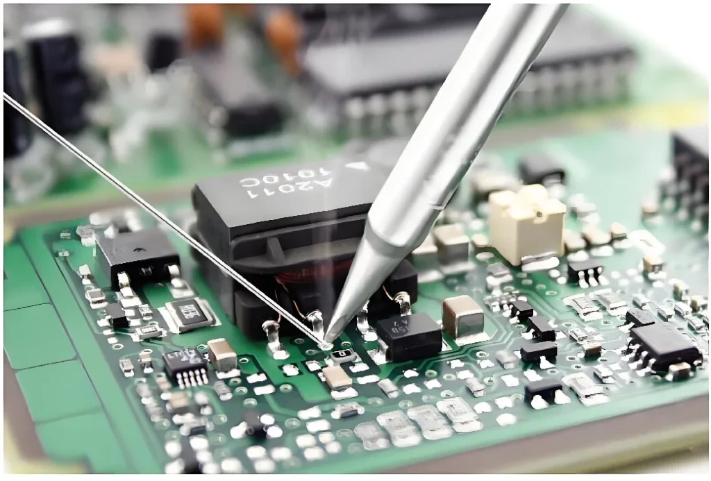
Printed circuit board production process
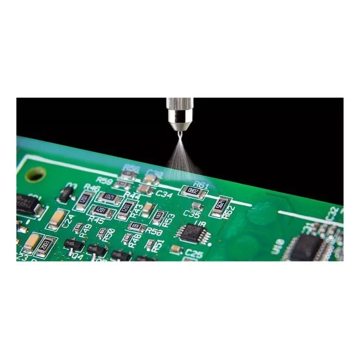
To design a printed board to meet the requirements of the diagram, electronic product designers need to have an in-depth understanding of the general flow of modern circuit board processing.
Single-Sided printed wiring board manufacturing process
Unloading → screen leakage printing → corrosion → removal of printed materials → hole processing → printing marking → flux coating → finished product.
double-sided printed wiring board manufacturing process:
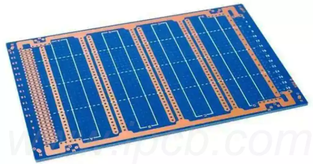
Printed circuit boards of various signal lines intricate, often forming cross, single-sided printed circuit boards can not meet, so there is a double-sided printed circuit boards, than the multilayer printed circuit boards are relatively inexpensive, most of the current printed circuit boards are still based on double-sided printed circuit boards.
(1) Process wire method
In the processing of double-sided printed circuit boards, in order to enhance the current-carrying capacity of the wire, to increase the wire part of the metal foil thickness. Usually after etching, all wire part of the copper plating.
Disadvantages: increase the coating process of peelable plastic, but also to the drilling of certain difficulties, affecting the quality of the hole. Wire widening. For line spacing small printed circuit board is not friendly. Is an imperfect backward process.
(2) Plug hole method
First of all, in the laminated metal sheet drilling the required variety of holes for hole metallization, and then plug all the holes with the plugging resist, and then the graphics transfer. Finally, clean up the hole resist.
Disadvantages: the whole board covered with copper, etching process burden increased etching dose, but also increase the etching time, and waste a lot of copper, affecting the quality of the printed circuit board mounted connection.
(3) Masking method
First of all, in the copper-clad plate according to the requirements of drilling a variety of holes, hole metallization, the entire copper-clad plate in the full-page copper plating, so that the copper layer reaches the required thickness. After the dry film resist for graphic transfer, to get a positive image of the circuit image. Dry film resist in the etching, on the one hand, to protect the circuit graphics, while also masking the metallization holes.
Disadvantages: full-board copper plating thickening, there is a waste of
(4) Graphic Plating Etching Method
After drilling holes for hole metallization, followed by graphics transfer to form a negative image circuit image. After developing, the concrete surface of the circuit graphic is exposed for plating, only the copper-plated part of the circuit graphic is thickened, and then plated with tin-lead alloy, making the copper plating partially protected. Drawing on the masking method plug hole method advantages, graphic accuracy, wiring density are relatively high.
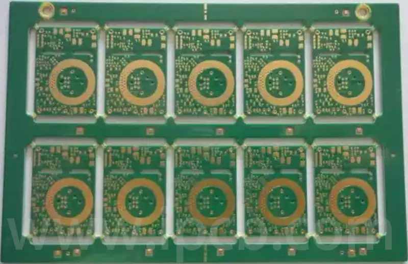
Disadvantages of the process is complex, wasteful, but still double-sided printed circuit boards, multilayer printed circuit boards, the main production methods.
(5) bare copper overlay soldering process SMOBC
Manufacturing high-density plated overlay holes commonly used in double-sided printed circuit boards. Eliminate the fine-pitch wires between the solder bridging short-circuit phenomenon, at the same time, due to a constant ratio of tin-lead, with better weldability and storage.
Printed circuit board development trend
Printed circuit boards from a single layer to the development of double-sided boards, multilayer boards and flexible boards, and constantly to high, high density and high reliability direction. Continuously reduce the size, reduce costs, improve performance, so that the printed circuit board in the future development of electronic products, still maintain a strong vitality.
Come to the circuit board processing and manufacturing technology development trend is in the performance to high-density, high, fine aperture, fine wire, small pitch, high reliability, multilayer, high-speed transmission, lightweight, thin direction.
The above is simple sharing from Mia, I hope it will be useful to you.