In modern electronic products, printed circuit boards (PCBs) are an indispensable core component. In order to ensure the performance and reliability of PCBs, the application of pcb solder resist is crucial. This article will explore various aspects of solder resist to help readers fully understand its importance in PCB manufacturing.

What is PCB solder mask?
The solder mask, also known as solder resist or Solder Resist, is an insulating protective coating covering the bare copper line of the PCB. Its main function is to prevent solder bridging, short circuits, and unnecessary wetting of the copper surface outside the pad during the soldering process. Visually, the solder mask often gives the PCB board a specific color, such as the common green, red, black, blue, etc. However, color is not just an aesthetic design, it also has a potential impact on visual inspection, light reflectivity, and signal integrity.
Material types and properties of solder mask
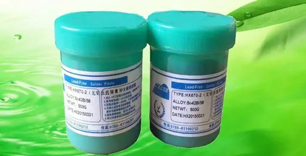
Currently, there are three main types of solder mask materials used in PCB manufacturing: liquid photosensitive solder mask ink (LPI), dry film solder mask (DFSM), and inkjet solder mask. Among them, LPI has become the mainstream choice due to its low cost and wide applicability. It is applied by screen printing or coating, and then the pattern transfer is completed through UV exposure and thermal curing process.
Dry film solder mask is mostly used in fine circuit boards because it has higher resolution and edge clarity, and is suitable for dense BGA and tiny pad structures. The latest inkjet solder mask technology is gradually being promoted. It directly prints graphics through digital inkjet, saves template costs and shortens production cycles. It is especially suitable for rapid proofing and small batch multi-variety PCB production.
PCB solder mask manufacturing process
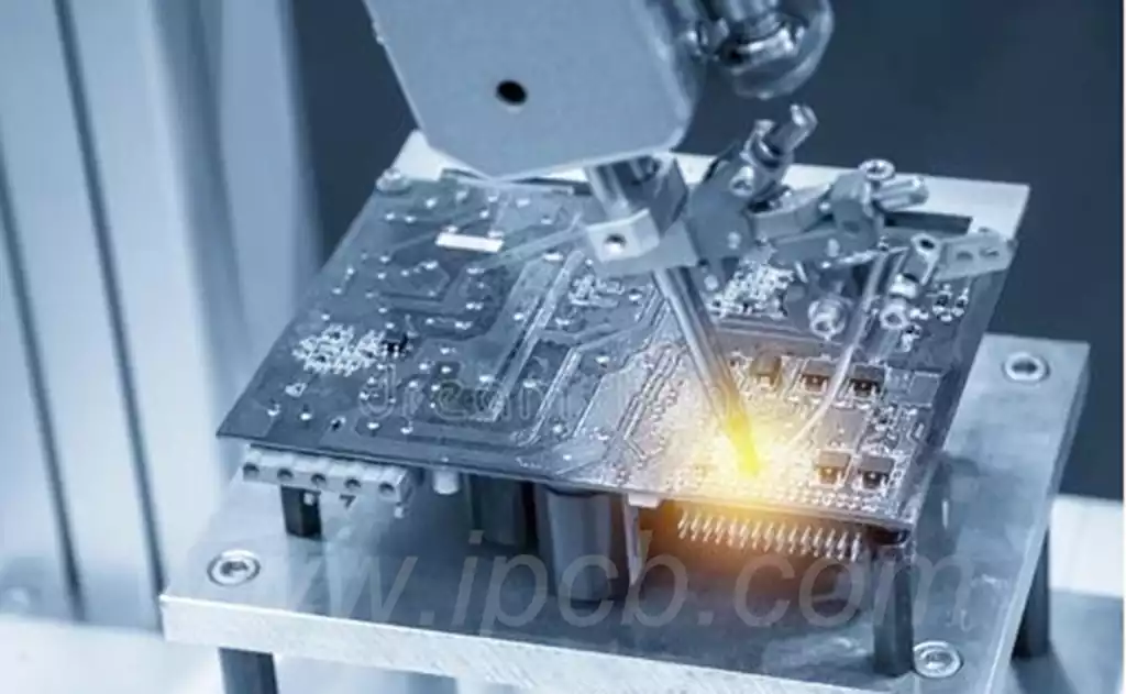
The manufacturing process of the solder mask is a highly precise process that requires close coordination between materials, equipment and process parameters. The manufacturing process mainly includes pre-treatment, dry film/liquid coating, exposure, development, curing and other steps. Each link directly affects the performance and appearance quality of the final solder mask.
The first step is the pre-treatment step, which usually includes decontamination, degreasing, micro-etching and other operations to ensure that the substrate surface has good roughness and adhesion. Then enter the coating stage. Depending on the solder mask material used, dry film lamination or liquid spraying technology is used. Dry film solder mask is mostly used for high-precision circuit boards because its edge definition is clearer; while liquid solder mask has the advantages of low cost and wide adaptability, and is more widely used in mass production.
After coating, the solder mask pattern needs to be cured and formed through UV exposure process. During the exposure process, the exposure energy and time must be strictly controlled to ensure that the pattern outline is clear and the solder mask edge is flat. Next is the development stage, and the unexposed part will be washed away by the developer to expose the pad area. Finally, the pattern is completely fixed by thermal curing or UV curing to improve its mechanical strength and chemical resistance.
Key points of solder mask quality control
In order to ensure the stability of the solder mask during PCB manufacturing and use, multiple quality controls must be performed during the manufacturing process. The focus of quality control includes indicators such as solder mask thickness uniformity, adhesion, development cleanliness, edge neatness, and chemical resistance.
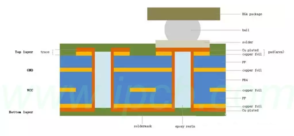
In terms of thickness control, the standard thickness range of general dry film solder mask is 15μm to 30μm, and that of liquid solder mask is 8μm to 20μm. Too thin can easily lead to pinholes and flying tin problems in subsequent electroplating or welding processes; too thick may cover the pad and affect the welding quality. Commonly used detection tools include laser thickness gauges and slice microscopic analysis
In terms of adhesion, peeling test, hundred-grid test and other projects are required to evaluate the bonding effect between solder mask and copper foil or substrate. If the adhesion is insufficient, the solder mask may fall off or crack during use, and even cause short circuit risk.
The problem of residual glue after development is also a common influencing factor. If the development process is not properly controlled, it is easy to cause residual solder mask to affect the exposed area of the pad, thereby affecting the welding effect. For this reason, it is generally combined with post-development cleaning and AOI inspection to ensure that the graphics are complete and free of residual glue pollution.
Future trends and technological innovations of solder mask
As electronic products develop towards smaller size, high integration, high frequency and high speed, the requirements for solder mask materials and processes are also increasing. Traditional green solder mask can no longer meet the needs of all emerging applications, so major material suppliers and PCB manufacturers are promoting multi-faceted upgrades in solder mask technology.
Solder mask adaptability at high frequency and high speed
In high-speed signal transmission scenarios such as 5G communications, automotive radars, and data center servers, signal integrity (SI) and electromagnetic compatibility (EMC) are particularly critical. The dielectric constant (Dk) and dielectric loss factor (Df) of solder mask materials cannot be ignored. For this reason, some high-end products have begun to use special solder mask materials with low Dk and low Df to reduce signal loss and improve overall circuit performance.
In addition, in order to avoid the irregular contours caused by traditional solder mask on the surface of high-speed lines, which leads to impedance discontinuity, manufacturers are also more inclined to use solder mask inks with better leveling and more uniform film thickness.
Challenges of flexible and rigid-flexible boards to solder mask
Flexible circuit boards (FPC) and rigid-flexible boards (Rigid-Flex) have been widely used in wearable devices, medical electronics and aerospace in recent years. Since the thermal expansion coefficient and adhesion characteristics of flexible substrates such as PI or PET are different from traditional FR-4, these circuit boards have higher requirements for the flexibility, adhesion and folding resistance of solder mask inks.
Developing solder mask materials with good flexibility and high adhesion performance has become the research and development focus of many ink manufacturers and PCB factories. For example, Japanese Sun Chemical, Korean Taiyo Ink and other companies have launched UV/thermal dual-curing inks suitable for FPC, which greatly improves the finished product reliability of flexible boards.
Diversification of solder mask colors and expansion of functions
In order to adapt to the appearance requirements, brand recognition and product identification (such as military and security boards), the color of solder mask has gradually expanded from a single green to black, white, blue, red, yellow, etc. Especially in applications such as camera modules, backlight LEDs, and mobile phone motherboards, white and black solder mask have become the mainstream.
However, it should be noted that the composition and optical properties of solder mask materials of different colors are different. White solder mask has strong reflectivity and is suitable for optical products, but its thermal stability and resolution control are also difficult; black solder mask has high light absorption, which helps prevent light leakage, but it is also more likely to cause over-curing or peeling risks due to heat absorption.
In addition, some advanced solder mask materials are developing in the direction of “functionalization”, such as composite solder mask coatings with anti-UV aging, anti-static, moisture-proof, and even thermal conductivity, which further extends the functional boundaries of PCB solder mask.
Intelligent and automatic detection of solder mask process
With the advancement of intelligent manufacturing, the traditional solder mask process that relies on manual inspection has also begun to integrate automation and AI technology. Modern solder mask lines can realize functions such as automatic adjustment of coating amount, online dry film lamination, and adaptive exposure compensation, thereby improving production yield.
In the solder mask detection link, new means such as AOI (automatic optical inspection) and laser profile scanning are introduced to effectively reduce common defects such as missing coating, foreign matter, bubbles, and oil interruption. Some PCB manufacturers have also established a solder mask thickness database to optimize parameter settings by tracing the solder mask film thickness records of the products, thereby realizing true digital closed-loop control.
Environmental regulations promote green solder mask materials
As global environmental regulations such as RoHS and REACH continue to tighten, clear restrictions have been put forward on solvent residues, harmful heavy metals and VOCs emissions in solder mask materials. This has prompted manufacturers to accelerate the development of low-volatile, halogen-free, and recyclable solder mask inks.
At present, some water-based solder masks and UV fully curable inks are gradually entering the commercial stage. Although their prices are slightly higher and the initial yield control is slightly more difficult, their environmental advantages and future development potential have become a market trend that cannot be ignored.
Summary
Although the solder mask is only a “thin coating” in PCB manufacturing, it plays a vital role. It not only protects the circuit from external pollution and oxidation, but also ensures the welding accuracy and reliability of the finished product. As electronic products tend to develop towards high density, miniaturization and high speed, the performance requirements of the solder mask are becoming more and more stringent, and its material selection, process control and quality management cannot be ignored.
From the diversification of colors and processes, to the adaptation of application environments such as high frequency and high speed, flexible boards, to the introduction of environmentally friendly materials and intelligent manufacturing, the solder mask is no longer just a “weldproof” tool, but a “comprehensive warrior” that combines functionality, structure and aesthetics.
In the future, with the continuous advancement of 5G, artificial intelligence, the Internet of Things and other fields, solder mask technology will also usher in new breakthroughs and innovations. As a PCB manufacturing engineer, purchaser or electronic industry practitioner, understanding and mastering the structure, characteristics and development trends of the solder mask will help you make more informed decisions in selecting materials, optimizing processes and controlling quality.
Remember: every layer on the circuit board, no matter how small, contains profound technical accumulation and manufacturing wisdom. The solder mask layer is the “green shield” that silently guards but is extremely critical.