In the field of electronics, the connector pcb edge plays a vital role in establishing a reliable and secure connection with external devices. Whether you are working on a computer, a game console, or any other electronic device, it is crucial to understand the importance of the connector pcb edge.
pcb edge connectors are also called gold finger connectors. Gold-plated pads are designed on the edge of the printed circuit board to fit into special sockets. The special application of these pcbs is to connect it to the motherboard or any additional storage device connected to the computer. High-speed and high-frequency signal applications adopt this pcb edge connection technology to ensure good connectivity of the signal.
For high-frequency signals, board-to-board connectors are more popular than board-to-wire or wire-to-wire connectors. The main purpose of using gold as the edge pcb connector metal is its durability and high conductivity. Generally, there are two types of gold plating, the first is soft gold or chemical nickel immersion gold (ENIG), and the second is electroplated hard gold. ENIG is usually 1U” or 2U” or 3U” thick, which is much thinner compared to hard gold. Hard gold thickness ranges from 20U” to 50U”.
Designing pcb edge connectors between the two edges of the pcb, using hard gold plating can improve conductivity and durability, preventing long-term wear. This allows the pcb to have more than 1000 pcb and connector mating times. Board cutouts are provided to help the pcb be fixed to the motherboard with rigid support.
Key features and considerations for selecting pcb card edge connectors:
- Connector type and form factor
Connector pcb edge has a variety of types and forms, such as single-row, double-row and multi-row configurations. It is necessary to consider the specific requirements of the project and select the connector type that meets the needs. Single-row connectors are suitable for applications with limited space, while double-row or multi-row connectors provide higher pin density for enhanced functionality.
- Contact Materials and Plating
The choice of contact materials and plating is critical to ensuring reliable and low-resistance connections. Common contact materials include phosphor bronze and beryllium copper. Choose connectors plated with gold, tin, or silver, as these materials offer excellent conductivity, corrosion resistance, and durability. Plating also helps prevent oxidation and extend the life of the connector.
- Insertion and extraction force
Consider the required insertion and extraction force of the connector. Connectors with the proper insertion and extraction forces ensure secure and easy-to-use connections. Connectors that are too loose, as they may cause intermittent connections, or connectors that are too tight, as they may cause difficulty in insertion and removal or damage the pcb, need to be avoided.
- Signal integrity and high-speed applications
For applications involving high-speed data transmission, it is imperative to select connectors that provide excellent signal integrity at the pcb edge. Look for connectors with impedance-matched designs and proper shielding to minimize signal loss, crosstalk, and electromagnetic interference (EMI). These features are critical to maintaining signal integrity in high-speed applications such as data centers or communications systems.
- Environmental Considerations
Evaluate the environmental conditions in which your electronic system will operate. If your project involves exposure to moisture, dust, or extreme temperatures, consider selecting a connector with appropriate sealing or protection features. Connectors with gaskets, shields, or rugged designs can help protect against environmental factors and ensure reliable performance even in challenging conditions.
- Durability and Lifecycle
Consider the durability and lifecycle of the connector, especially if your application requires frequent insertion and removal. Look for connectors designed for high mating cycles to ensure long-lasting performance and reduce maintenance requirements. Connectors with reinforced contacts or rugged housing materials can withstand the rigors of frequent use, making them ideal for applications that require reliability and durability.
- Compliance and Standards
When selecting connector pcb edges, make sure they comply with industry standards and regulations. Look for connectors that meet or exceed specifications such as IPC standards or RoHS compliance. Meeting these standards ensures that the connector is manufactured to high-quality standards and is suitable for a wide range of applications.
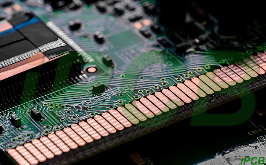
The connector pcb edge is an important component in establishing a reliable and secure connection between the pcb and external devices. Correctly selecting the appropriate specifications will help improve the overall performance, reliability and service life of the electronic system.
The edge of the connector pcb used in certain applications must provide a guaranteed electrical connection for power transmission when used in an environment with a temperature of 200-350°C for a long time. It is required to provide a connector that can be mounted on a circuit support substrate such as a thin metal plate coated with ceramic, and the electrical connection with its circuit should ensure long-term application at high temperatures such as 200-350°C, and a complementary connector can be matched with it to perform power transmission of, for example, 5-15A.
It is a connector with one or two contacts for electrical connection with various circuits of a circuit support substrate, which can be easily assembled to the substrate without special process equipment, and thereafter maintains a reliable electrical connection between the contact and the circuit even during long-term application in a high temperature environment for power transmission. Openings through the substrate, such as notches along the edge of the substrate wing, or holes through the substrate can be used, and parts of the connector base or clamping member are arranged through these notches or holes to establish mechanical fixation of the connector in a way that fixes the connector to prevent it from translation and rotation. The elastic part of the connector generates a considerable force that pushes the substrate onto the contact for electrical connection. The substrate can be a thin metal plate coated with ceramic, or it can be a circuit board or other circuit support.
Classification of Edge pcb Connectors
pcb edge connectors or gold fingers are divided into three types based on design aspects, namely:
Conventional gold fingers: Conventional gold fingers are standard gold finger design practices, with equal pad lengths and symmetrical distribution on the edge of the pcb. These designs are used for graphics cards, network equipment, etc.
Segmented gold fingers: The segmented gold fingers are arranged similarly to the general gold finger circuit, and a few pads are designed with small gaps to electrically separate the connections.
Long and short gold fingers: Unlike conventional or segmented gold fingers, the height of the gold pads is uneven. They are used in applications such as USB drives, memory cards, and card readers.
Advantages of edge pcb connectors
- Gold finger connectors are used to connect cards, PCle, PCI, USB, and storage devices to another board.
- Edge pcb connectors are placed on the edge of the circuit board, eliminating the need for external manual connectors and saving on harness costs
- Gold fingers are more conductive and hard gold is durable, providing excellent performance after multiple plugging and unplugging.
- Edge pcb connectors are designed as pads with chamfered edges to achieve matching and complete mating. They are mounted on the top of the connector to form electrical contact points.
- Continuous plugging and unplugging of pcb edge connectors is very reliable and does not cause any major damage to the contact points. Once mated with the connector, the rigidity of the pcb provides a solid support for the pcb.
- Although gold is an expensive plated metal, it performs better, saves on component and harness costs, and reduces the size of the entire product to a compact size.
Applications of Connector pcb Edge
Connector pcb Edge is widely used in many industrial fields, especially in industrial equipment, computers, and laptops. We list some:
Telecom applications for USB and HDMI cables to connect laptops or pcbs.
Storage devices such as SD cards, graphics cards, etc. in cameras use Edge connections.
Advanced industries use pcb edge connectors for high-speed, high-precision applications
Design rules for board edge connectors
The electrical connection is located at the edge of the pcb, so certain standards must be followed to meet design needs. Regardless of the application of the pcb edge connector, there are some standard rules that must be followed, which are: - The spacing between the edge of the connector and the edge of the pcb board connector must be at least 0.5mm.
- Surface mount devices, through holes and pads should be at least 2mm away from the gold fingers.
- The chamfering process on the edge of the pcb may expose the internal copper layer, so it must be removed during the design stage to avoid unwanted contact. There are two processes for removing copper: full-finger removal or half-finger removal. Removing copper helps control the impedance in the gold fingers and provides ESD (electrostatic discharge) protection.
- The height of ordinary gold fingers should not exceed 40 mm, because the board edge connector on the motherboard does not need to exceed this height.
- The design should have a solder mask opening along the edge of the pcb.
- Through-hole vias using the plated manufacturing process should not be placed near or on the board edge connector.
- The gaps of these gold fingers should be kept with a certain clearance from the solder mask and silk screen to avoid overlap
- The edges of the pcb are beveled, so the gold fingers must be placed in opposite directions
- The chamfers on the connector edges are set to avoid breakage and weakened connections. The standard design has an angle of 45 degrees, and in a few applications, the angle can be adjusted according to the connector design specifications.
If the design rules are not adapted to the pcb design, it can cause electrical and mechanical stress. The purpose of using hard gold instead of nickel, copper or other alloys is because its properties are to provide higher strength and conductivity. The design must mention the thickness of gold. Although gold is one of the most expensive metals, it is used because it makes proper contact with the pcb board edge connector and is corrosion-resistant, ensuring a longer life of the pcb.
Manufacturing standards for connector pcb edges
The Institute for Printed Circuits (IPC) standards provide a specific set of guidelines for designing pcb edge styles. The IPC standards cover all attributes that ensure quality during the manufacturing process. - The chemical composition of gold should contain 3% to 15% cobalt, depending on the thickness, which ensures rigidity of the pcb edge.
- Gold thickness can be classified as hard gold and soft gold. Soft gold is usually 1 U” to 3 U” while hard gold can go up to 50 U”. Soft gold material is used for initial prototype testing and for a few applications where the mating cycle is not long. After hard gold plating, the mating cycle is checked with the edge of the connection for proper mating cycle.
- Optical inspection is done by AOI (Automated Optical Inspection) machine and manual micro lens to ensure finish and clearance.
- IPC recommends a tape test where the tape is stuck to the edge of the pcb and then removed. This ensures that the bond between the gold finger and the substrate is strong and the traces and solder mask are not falling off.
The gold plating process is done after the solder mask process. The connector pcb edge pads are nickel plated 1 U” to 3 U” to improve reliability and adhesion with gold. After hard gold plating, a small amount of cobalt mixture is added to the composition. The gold plated fingers are beveled before being sent for inspection.
