In the production process of electronic products, the quality of PCB design directly affects the reliability and performance of the final product. Welding as a key link in the PCB assembly process, the requirements of the design stage is particularly important. The following will be talked about from the welding point of view, design PCB need to pay attention to what issues:
PCB welding quality influencing factors.
From the beginning of the PCB design stage, until all components are successfully welded to form a high-quality circuit board, the entire process requires PCB engineers, welding process and welding workers to work together and strict control.
The main factors affecting the quality of soldering include: PCB design, the quality of the board itself, the quality of the device, the oxidation status of the device pins, the quality of the solder paste and the printing effect, the accuracy of the bonder programme, the level of placement of the bonder, and the temperature control curve of the reflow oven.
For soldering factories, the accuracy of PCB design drawings is a key aspect that they cannot avoid.
Usually, circuit designers are seldom directly involved in circuit board soldering work, and therefore lack of rich practical experience in soldering; while the workers in the soldering factory are focused on production tasks, do not know much about PCB design, and lack the ability and willingness to analyse the causes of poor soldering. These two sides of the talent each take on different responsibilities, it is difficult to form an effective co-operation and integration.
Suggestions when drawing PCBs
The following are some suggestions aimed at avoiding the generation of bad designs that affect soldering quality.
1.On the design of positioning holes
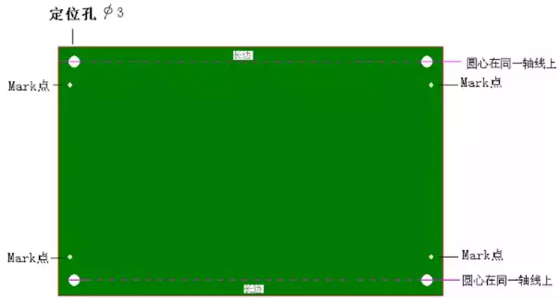
It is recommended to reserve a hole (minimum hole diameter of 2.5mm) in each of the four corners of the PCB board. The main purpose of these holes is to be able to accurately position the board when printing solder paste. Requirements for these holes in the X-axis or Y-axis direction, the centre of the circle should be located in the same straight line.
2.On the design of MARK point
Mark points must be included on the PCB board, this is for the mounter to be able to accurately locate them.
Specific location selection: Mark points should be set in the diagonal position of the pcb board, can be round or square pads, but must ensure that they will not overlap with other device pads or confused. If there are devices mounted on both sides of the PCB, then both sides need to be marked with Mark points.
In addition, you can also consider adding MARK points to the collocation as well to improve the accuracy of positioning.
3.During the PCB design process, please pay attention to the following points:
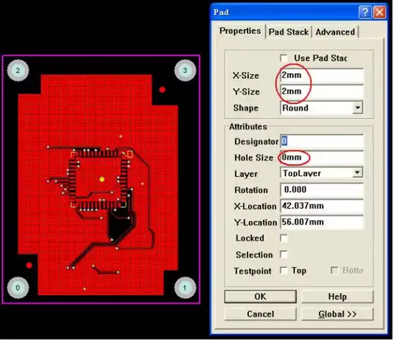
a. The design of Mark points can refer to the following pattern, which requires the shape to be symmetrical up and down or left and right.

b.The diameter of Mark point A shall be set to 2.0mm.
c.Within a range of 2.0mm from the outer edge of the Mark point, the presence of any shape variations or colour differences that may interfere with accurate identification should be avoided, including pads and solder pastes.
d. In order to ensure that the Mark point can be clearly identified, its colour should form a clear contrast between light and dark with the colour of the surrounding PCB board.
e.To enhance the accuracy of identification, the surface of Mark points should be plated, such as copper or tin plating, to prevent identification troubles caused by light reflection. It should be noted that Marks consisting only of lines cannot be recognised by the light point recognition system.
4.Recommendations on edge allowance dimensions
When designing a PCB, make sure that you leave at least 3mm of edge space in the longitudinal direction, this is for the mounter to be able to transport the board smoothly. The mounter will not be able to place devices within this margin, so it is not recommended to place any devices within this margin. For boards with components on both sides, problems such as component removal and pad damage need to be taken into account when planning the secondary reflow process.
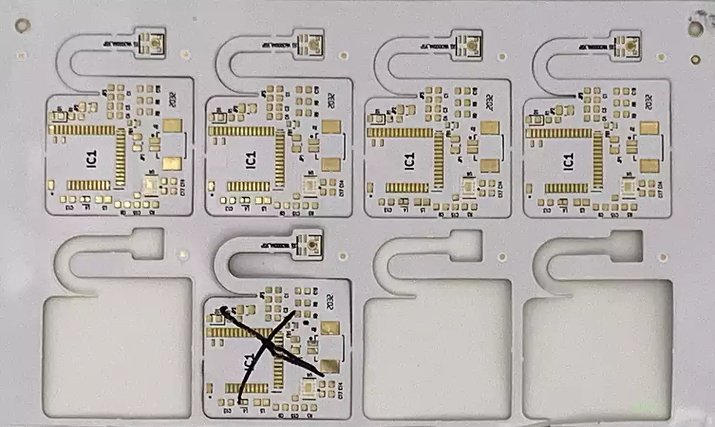
It is recommended to avoid arranging SMD components within 5 mm from the edge on the long side on the side with fewer chips. If it is difficult to avoid due to limited space on the board, you can consider increasing the process edge on the long side as a solution.
5.Avoid drilling holes directly on the pads
If holes are drilled in the pads, solder paste may flow into the holes during the reflow process, resulting in a lack of solder in the device pads, which may lead to soldering problems.
6.Polarity labelling specifications for diodes and tantalum capacitors
The polarity labelling of diodes and tantalum capacitors should strictly comply with industry standards to avoid workers soldering in the wrong direction due to reliance on personal experience.
7.Suggestions on silkscreen and labelling treatment
It is recommended to hide device type information, especially on boards with dense device layouts.This avoids visual confusion and facilitates fast and accurate positioning of soldering locations.At the same time, should also avoid only marking the model number and ignore the marking,as shown in the figure, this practice will lead to the mounter in the programming can not be carried out smoothly.The size of the silk-screened characters should be kept from being too small, and the characters should be placed in such a way that they do not overlap with the over-holes to prevent confusion or errors when reading.
8.On the extension of the IC pad design
For SOP, PLCC, QFP and other packages of IC, it is recommended that the length of the pad on the PCB is designed for the length of the IC foot 1.5 times, this design facilitates the use of soldering iron for manual soldering to ensure that the chip foot, PCB pad and tin can be fully fused into one.
9.On the IC pad width design
In drawing SOP, PLCC, QFP and other package types of IC corresponding to the PCB, you need to pay special attention to the width of the pad. Specifically, the width of pad a on the PCB should be consistent with the width of the IC foot (i.e., the nominal value Nom. in the datasheet), and additional widening is usually not recommended. Doing so ensures that the spacing b between the two pads is spacious enough to effectively avoid possible contiguous soldering during the soldering process.
10.Device placement should follow standard angles
Since the mounter only supports 90°, 180°, 270° and 360° rotations, arbitrary non-standard angles should be avoided when placing devices.For example,if the device is rotated by 1 °, after mounting, the device pin will form a 1 ° deviation from the pads on the circuit board, and this deviation will adversely affect the quality of soldering.
11.Design points on the short connection of adjacent pins
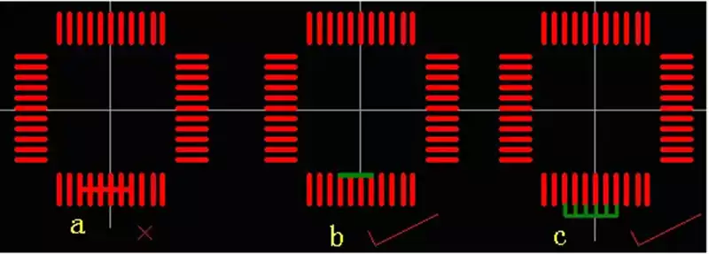
Adopting the shorting method as shown in Fig. a will not only make it more difficult for workers to identify,but also the appearance of the finished soldering will not be satisfactory.
On the contrary, if the shorting is done at the time of design according to the method in Fig. b or c and the solder resist layer is added,then the result of the soldering will be significantly improved.
It is important to ensure that each pin is independent of each other, no short-circuit phenomenon, at the same time, such a design can also make the circuit board looks more neat and beautiful.
12.Optimising the design of the central pad on the bottom of the chip
For chips with a protruding part (commonly known as the ‘belly’), it is recommended that the design size of the central pad be appropriately reduced to increase the distance between it and the surrounding pads, thereby reducing the risk of short-circuit.
13.Avoid high thickness devices closely arranged
If two devices with high thicknesses are arranged close together, the second device may collide with the previously mounted device when it is placed on the bonder. This collision will be detected by the machine as a dangerous situation, which will lead to automatic machine power failure, affecting production efficiency.
14.Special Precautions for BGA Packages
In view of the special characteristics of the BGA package, the pads are all hidden at the bottom of the chip, so it is not possible to directly observe the soldering effect.
In order to facilitate the subsequent rework work, it is recommended to set up two positioning holes on the PCB board, the aperture size of 30mil, in order to be able to accurately locate the stencil during rework.
Special note: the size of the positioning holes should be designed to ensure that the insertion of positioning pins will not fall off or wobble, but also have a certain degree of tightness, but should not be too tight. If the size is too large or too small, may lead to inaccurate positioning, affecting the rework effect.
15.Recommendations on the choice of PCB board colour
It is recommended to avoid using red as the colour of PCB board. This is because red circuit boards will appear white when illuminated by the red light source of the mounter camera, which will result in the inability to perform effective programming, thus causing inconvenience to the soldering work of the mounter.
17.The effect of copper cladding and pad connection on solder melting
The copper cladding area absorbs a lot of heat due to its good thermal conductivity, which can cause difficulties in melting the solder to reach a completely molten state, which may lead to soldering problems.

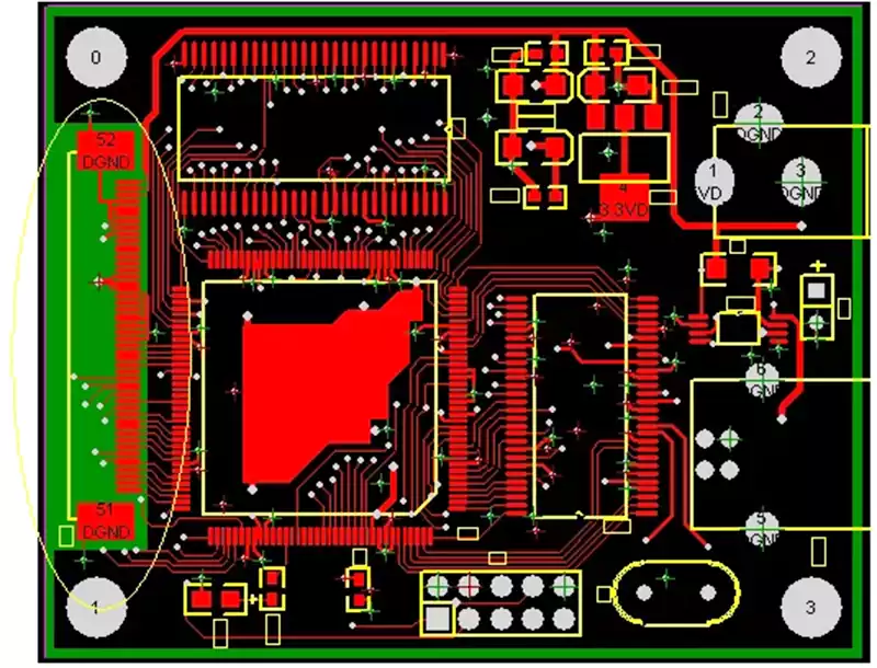
In Fig. a, the pads of the device are directly connected to the copper cladding area; whereas in Fig. b, although the 50Pins connector is not in direct contact with the copper cladding, the solder paste is not sufficiently melted due to the fact that the middle two layers of the four-layered board are covered with a large area of copper, as is the case in both Fig. a and Fig. b, because of the large amount of heat absorbed by the copper cladding area.
Of particular note, the 50Pins connector body in Figure b is made of plastic that is not resistant to high temperatures. If the soldering temperature is set too high, the plastic body of the connector may melt or be deformed; while if the temperature is set too low, the solder paste will not be able to melt sufficiently because the copper cladding absorbs a lot of heat.
Therefore, in order to avoid these problems, it is recommended to isolate the pads from the large copper cladding area, as shown in the diagram:
