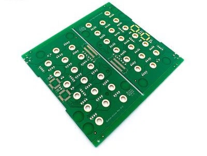
Copper Coin PCB, as the name suggests, is a technology that embeds copper coins into PCB boards. This copper coin is actually a solid piece of copper that is skillfully embedded into the PCB and tightly connected to key components.
The main advantage of copper coin PCB is their excellent thermal conductivity. As an excellent thermal conductive material, copper is able to quickly conduct heat away from the component generating the heat and emitting it to the outside world through a heat sink, thus effectively preventing overheating of the component.
Compared with traditional heat dissipation methods, it has higher heat dissipation efficiency and lower energy consumption. Since it conducts heat directly from the component without the need to dissipate heat through air convection or liquid circulation, it has a higher heat dissipation efficiency. It also reduces energy consumption and noise in electronic devices because it reduces the use of cooling devices such as fans.
Copper Coin PCB also has a higher degree of integration and smaller size. As it perfectly combines the heat dissipation function with the circuit board, it makes the internal structure of electronic devices more compact and reduces the occupied space. This is undoubtedly a huge advantage for the pursuit of thin and light portable electronic devices.
Embedded copper block multilayer pcb board process flow
Opening (copper block, FR4 substrate, semi-cured sheet) → inner layer line → inner layer AOI → OPE punching → inner core board and semi-cured sheet milling slot → browning → riveting → pressing (placing the copper block) → chipping overflow glue (milling board) → milling blind groove (controlled depth milling machine) → mechanical drilling (including drilling blind holes) → chemical copper-plating → board electricity → outer layer line → graphic plating → outer layer etching → outer layer AOI → anti-soldering → text → molding → electrical testing → chemical tinning → finished product Electrical testing →chemical tinning →finished product inspection →packaging out of the warehouse
Embedded copper block high-frequency mixed compression plate process flow
Opening (copper block, FR-4 substrate, high-frequency substrate, semi-cured sheet) → inner layer line (including high-frequency board) → inner layer AOI → OPE punching → inner core board and semi-cured sheet milling slot → browning → riveting → pressing (placing the copper block) → chipping overflowing adhesive (milling board) → mechanical drilling (including drilling blind holes) → chemical copper-plating → board electric power → outer line → graphic plating → outer layer etching → outer layer AOI → anti-soldering → text → molding Slot milling → chemical nickel/gold plating → molding → electrical testing → finished product inspection → packaging out of the warehouse
Manufacturing key technology and control measures
Copper block molding
There are three main methods for copper block molding: the first is to mill the required size of the copper block directly through a special milling machine, but it needs to be equipped with a metal substrate milling machine, a special milling cutter, and the cost is high; the second is to be processed through the milling machine secondary milling machine with the function of controlling the depth of the milling machine, the use of drill-tip shaped double-edged milling cutter rough milling once, and then finish milling once, but it needs to be equipped with a milling machine with the function of controlling the depth of the milling machine, special milling cutter, and the cost is high; the third one is to The third is to use the punch cutting, although high production efficiency, but the mold production cost is high, poor production flexibility, is not suitable for prototype or small batch production. To solve the above problems, developed a graphic etching and milling process, the first copper block graphic transfer, and then through the etching machine etching out the copper block shape, and then use conventional milling cutter, milling machine on the shape of the copper block for the secondary processing, so the production efficiency is higher, the production cost is relatively low.
Copper block pressing
Before copper block press-fitting, the copper block should be browned horizontally and browning aids (e.g., mesh mopping) should be used to prevent the copper block from being too small in size, resulting in the machine jamming the plate or dropping it into the cylinder, and to ensure that the copper block is micro-etched. In order to improve the flatness and reliability of the copper block and plate (or mixed pressure area), in addition to the need to consider the match between the thickness of the copper block and the thickness of the plate, but also the selection of suitable cushioning materials such as release film, aluminum, cushioning pads, and the order of press-fit platings (Figure 6). The design of the stacked structure is further optimized by selecting semi-cured sheets with high resin content, and setting up a special press-fit program for buried copper block PCBs so that the resin is fully filled and the material is fully cured to ensure heat resistance and insulation after press-fit.
Steps of PCB buried copper process to make PCB circuit board:
1.Design schematic diagram of pcb and generate Gerber file.
2.Fabricate the PCB sheet and cover the copper foil on the fiberglass substrate.
3.Apply light sensitive coating to the PCB sheet and then expose the Gerber file to the coating through an exposure machine.
4.Place the exposed PCB sheet into the developer so that the unexposed photosensitive coating is dissolved away, exposing the copper foil.
5.Place the PCB sheet into the etching solution so that the exposed copper foil is etched away to form the shape of the circuit diagram.
6.Clean the PCB to remove the photosensitive coating and etching solution.
7.Coat the PCB with copper embedded coating, and then put the PCB into a high temperature and high pressure pressing machine, so that the copper embedded coating is combined with the copper foil.
8.Drilling, plug-in installation, soldering and other subsequent processes on the PCB board.
9.Conduct electrical testing and quality inspection to ensure that the quality of the PCB board meets the requirements.
As a new type of heat dissipation technology, Copper Coin PCB provides a new solution to the heat dissipation problem of electronic devices. Its excellent thermal conductivity, high efficiency of heat dissipation and compact size make it has a broad application prospect in the field of electronic equipment heat dissipation.