High frequency pcb and high speed pcb belong to the same PCB circuit boards used for signal transmission, however, there are significant differences between the two in the actual application scenarios, mainly reflected in the following.
Frequency band application differences: high frequency pcb focus on frequency bands above 500MHz, specifically to cope with high-frequency signal transmission needs; high speed pcbs focus on the field of digital signal transmission, and its modulation and demodulation frequency range across dozens of MHz to GHz level, the two have their own focus on the frequency band coverage.
Line geometry differences: high frequency pcb need to use micro-fine line design, its line width, line spacing is significantly smaller than the high speed pcb, the board thickness is relatively thin, in order to adapt to the high-frequency signals on the line accuracy of the stringent requirements; high speed pcbs through the optimisation of the line isometric design, can be appropriate to relax the parameters of the line width, line spacing, and moderately increase the thickness of the board, in order to ensure the integrity of the signal and take into account the feasibility of the processing.
Difference in substrate characteristics: high frequency pcb use materials with lower dielectric constant to reduce signal transmission loss, typically represented by PTFE (polytetrafluoroethylene), its low dielectric constant and low-loss characteristics of the high-frequency application requirements; high speed pcbs use FR4 high TG materials, FR-4 (glass fibre covered with copper) and other upgraded substrate materials, such as these materials in the performance of the dielectric properties, anti-jamming capabilities and signal delay control performance These materials have excellent performance in dielectric properties, anti-interference ability and signal delay control to meet the precision requirements of high-speed digital signal transmission.
Manufacturing process differences: high frequency pcb production process precision requirements are extremely high, need to ensure that the outer surface is absolutely flat to carry micro-fine conductive materials, the inner layer of the copper process needs to control the thickness of the copper layer in a few microns, the entire production process needs to use special techniques and strict quality control measures; high speed pcb manufacturing process is relatively simplified, the conventional drilling and cutting equipment to meet the production requirements, and the later through the completion of high-precision mechanical machining plate Forming, focusing on the need to avoid physical damage to the circuit processing and electromagnetic interference.
Design considerations: high frequency pcb design to optimise the physical characteristics of the core, you need to focus on controlling impedance matching, surface roughness, material adhesion and conductivity and other parameters; high speed pcb design focuses on signal integrity protection, you need to accurately calculate the signal delay (TDR) and differential signal amplitude and other indicators, through the simulation and parameter optimisation to achieve a stable transmission of high-speed signals.
In practical applications, according to specific technical indicators and application scenarios, we need to select high frequency pcb or high speed pcbs to ensure the stability of product performance and the reliability of signal transmission.
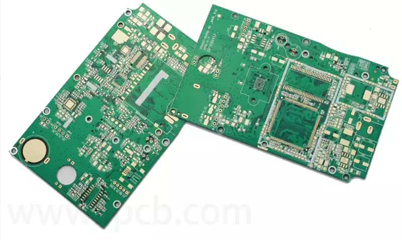
High speed pcb is used in data transmission, such as networks, computer motherboards, industrial control machines, measurement and control instruments and high-speed memory and other fields. Focusing on data transmission, its main requirement is to maintain signal integrity, stability and high accuracy. high speed pcbs are generally used in areas such as high-speed differential signals, coaxial cables and serial communications. Due to its better line isometry, it ensures better signal integrity and interference immunity when transmitting high-speed digital signals.
High frequency pcb is widely used in wireless communications (such as mobile phones, satellite communications), radar systems and antennas and other fields. Its main role is to help the transmission of high-frequency signals and transmission accuracy. Due to the use of microfabricated lines, it can reduce phenomena such as signal attenuation and crosstalk and enhance the output power of the circuit signal, improve the transmission rate and reception sensitivity, and have very good transmission and reception characteristics.