Differential signal line is mainly the difference between the traditional signal line corresponds to a ground line signal transmission mode, differential signal transmission is mainly two lines on the signal transmission, the two signals are equal in amplitude and opposite in phase. Relative to the traditional single-ended signal, it has a strong anti-jamming, can effectively suppress electromagnetic interference and timing positioning preparation and other advantages.
In circuit board design, differential signal wiring need to pay attention to two aspects:
(1) The length of the two lines should be as consistent as possible.
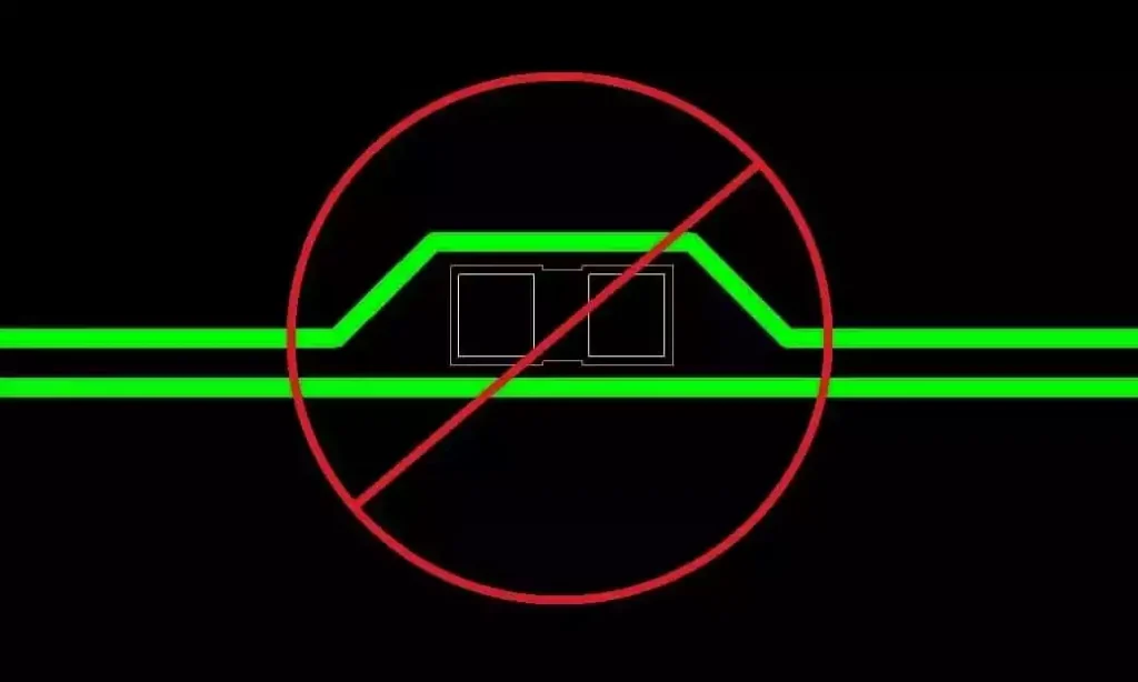
(2) The spacing between the two lines should always be fixed, the spacing is determined by the differential impedance, and should be kept parallel.
Parallel alignment is usually done in two ways: one is when two lines are located in the same signal layer (side-by-side alignment), and the other is when two lines are located in the upper and lower neighbouring layers (upper and lower alignment); the same-layer side-by-side approach is more common. Differential signal lines are only valid when both the source and receiver are differential signals, so for clock signals with only a single output, differential signals lines cannot be used. It is common to put matching resistors between the differential lines at the receiving end, with a resistance equal to the differential impedance, to improve the signal quality.
Differential signal lines need to be close together and parallel because the distance between the lines directly affects the differential impedance, which is a key parameter in the design of differential pairs. Maintaining parallelism ensures that the differential impedance is consistent; if the line spacing is too large or too small, it will lead to impedance discontinuity, affecting signal integrity and timing delay.
The following specifications should be followed in specific applications:
SDRAM clock signals
Due to the high clock frequency (≥75MHz), the wiring length should be controlled within 1000mil to avoid the transmission line effect; the line width is recommended to be 10mil, with an internal spacing of 5mil, and an external spacing of 30mil. Differential pairs of alignments need to be matched accurately with a length error of no more than 20mil, and to avoid crosstalk with the neighbouring signals. Crosstalk.
Address, chip select and other control signals
The line width is set to 5mil, internal spacing is 10mil, external spacing is 12mil, and the alignment form is mostly daisy-chain topology, which can effectively inhibit the high harmonic interference, and the length of the line can be longer than that of the clock line, but should not be shortened.
SDRAM data line
line width of 5mil, internal spacing 5mil, external spacing 8mil, it is recommended that the same layer of wiring, and data lines and clock line length difference control within 50mil.
For high-speed differential signals (generally more than 5Gbps), interference and jitter is extremely sensitive, so in the wiring should be selected with excellent performance of microstrip or ribbon cable to ensure that the impedance of the entire signal path is consistent. When designing, be sure to first determine the laminated structure to ensure that the alignment can accurately match the impedance.
Due to the very high frequency of high-speed differential signals, the length of the differential line must be strictly matched, the length of the mismatch will introduce common-mode noise, radiation and even serious timing jitter problems. Taking 6.25Gbps signal as an example, the code element length is only about 160ps, and the microstrip line transmission speed on FR4 PCB is about 180ps per inch, so the 50mil alignment difference may bring about about 9ps timing offset. The 50mil uncoupled length allowed in low-frequency designs can trigger timing errors in high-speed applications. Therefore, maintaining a tight length match is a top priority for high-speed differential pair alignment design.
Specific Steps for Differential Pair Alignment
- Create the Differential Pair Network: In PCB design software, you first need to define the differential pair network. This usually involves setting the name of the differential pair and the contained network.
- Set the rules of the differential pair: In the design rules, set the specific rules of the differential pair, such as alignment width. Spacing. Hole size, etc.
3.Start Alignment :Use the Differential Pair Wiring tool to start alignment. During the wiring process, the software will display the wiring length and difference in real time to ensure that the length of the two wires are as equal as possible. - Adjust the alignment: In the wiring process, it may be necessary to adjust the PCB space layout and other design requirements. Use the software’s editing tools to optimise alignment paths and shapes.
- Check and optimise: After completing the alignment, use the design rule checking tool to check whether the differential pairs meet all the design requirements. For the parts that do not meet the requirements, perform the necessary optimisation.
Advanced Tips and Notes
Impedance Matching: Ensure that the impedance of the differential pair is consistent throughout the entire signal path, including the alignment, vias, and connectors.
Shielding and grounding: Provide shielding for differential signals as much as possible, and ground them correctly at the receiving end to effectively reduce EMI.
Heat management: Focus on the heat dissipation design of the PCB to prevent differential signals from overheating and causing performance degradation.
Signal Integrity Assessment: Predict and optimise the transmission performance of differential pairs at the design stage through signal integrity analysis tools.
The scientific design of differential signal wiring is critical to ensure high-speed, high-quality signal transmission. By strictly controlling wire length matching and spacing stability, combined with reasonable layer stacking structure and impedance matching, signal integrity can be effectively improved, and interference and timing errors can be reduced. At the same time, reasonable shielding and grounding and thermal management measures should not be ignored to help ensure the stability of differential signal performance.