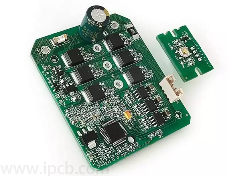
In the field of electronic manufacturing, double-sided PCB board assembly by virtue of its high integration, small size and other advantages, widely used in various types of electronic products, from smart phones, tablet computers to industrial control equipment, automotive electronic systems, are inseparable from its figure. It can not only effectively save board space, but also enhance the performance and reliability of electronic products. However, double-sided PCB board assembly process is complex and delicate, involving a number of key links, any one step of negligence may lead to product quality problems.
Detailed process of double-sided PCB board assembly
Incoming Material Inspection: Strict quality inspection of PCB boards, components and other materials to ensure that there are no defects and damage.
A-side processing
Solder Paste Printing: Use a stencil to accurately print solder paste onto the A-side pads of the PCB.
SMD: Accurately place the required SMD components on the A-side of the PCB through the SMD machine to the specified position.
Drying and curing (if using SMD adhesive): Dry and cure the SMD adhesive to ensure that the components are fixed.
Reflow Soldering: Send the PCB board with the pasted components into the reflow oven for soldering to form a solid solder joint.
B-side processing
Flip board: Place the finished soldered A-side face up, ready for B-side processing.
Solder Paste / Patch Adhesive Coating: According to the type of components on the B-side, choose to apply solder paste or patch adhesive.
Placement: Place the required components on the B-side through the placement machine to the specified location precisely.
Drying and curing (if applicable): Dry and cure the patch adhesive on the B-side.
Reflow or Wave Soldering: Depending on the type of B-side components, reflow or wave soldering is selected for soldering. For through-hole inserted devices, wave soldering is usually used.
In addition, for a circuit board with more BGA and IC devices, because of the need to eliminate certain dropouts and solder reflow problems, so the important devices will be placed on the second side of the hit, so that it is only once through the reflow oven. For other fine foot components, if the DFM allows the case can be the first side of the first mount, so it will be placed on the second side of the mount for the precision of the control is better. Because when the PCB circuit board in the first back to the soldering furnace, the impact of high-temperature soldering will occur under the influence of the naked eye can not be seen, but affects part of the tiny pin welding bending and deformation, at the same time it will cause the solder paste printing to produce a small offset, and the second amount of solder paste is difficult to control.
Cleaning and Inspection
Cleaning: Remove the solder paste, flux and other impurities left in the soldering process.
Appearance Inspection: Use automatic optical inspection equipment (AOI) or manually check the quality of the solder joints, the position and direction of the components.
Functionality test: Electrical performance test on double-sided PCB boards to ensure normal function.
Rework and Packaging
Rework: Rework the problems found in the test to ensure product quality.
Packaging and shipping: qualified products are packaged and ready to be shipped to customers.
Precautions in PCB board assembly
- Work environment control
Cleanliness: Keep the work shop and workbench clean to prevent dust, impurities and other pollutants from entering the board.
Temperature and humidity control: Maintain appropriate temperature and humidity to reduce the generation of static electricity and the impact on electronic components.
- Static electricity protection
Electrostatic damage to electronic components is invisible but serious consequences, so operators should wear anti-static clothing, anti-static bracelets, workstations and equipment should be well grounded. - Component management
Classification and storage: different specifications, models of components should be classified and stored, and well marked.
Placement order: Reasonable arrangement of the placement order of the components to improve the efficiency and quality of the patch.
- Welding quality control
Temperature and time control: Reasonable setting of welding temperature and time to avoid damage to components and circuit boards.
Welding quality check: Make sure that there is no false welding, fake welding, continuous welding and other bad phenomena at the welding point.
- Paste sequence
When dealing with double-sided PCB board assembly, the placement sequence should be reasonably arranged, usually starting from the low component, and gradually transitioning to the taller components, in order to avoid collision and displacement during the placement process.
Double-sided PCB board assembly as a key process in electronic manufacturing, the process interlocking, rigorous and meticulous, each step carries an important mission to ensure product quality and performance. In the rapidly changing electronic technology, market competition is becoming more and more intense, only down-to-earth to follow the process, pay attention to detail, in order to do a good job of double-sided PCB assembly, for the stable operation of electronic products to provide reliable support, in the steady development of the industry to contribute to the solid power.