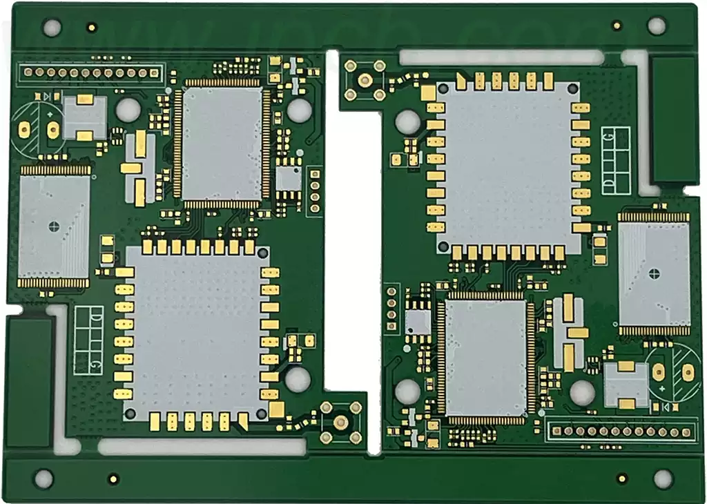
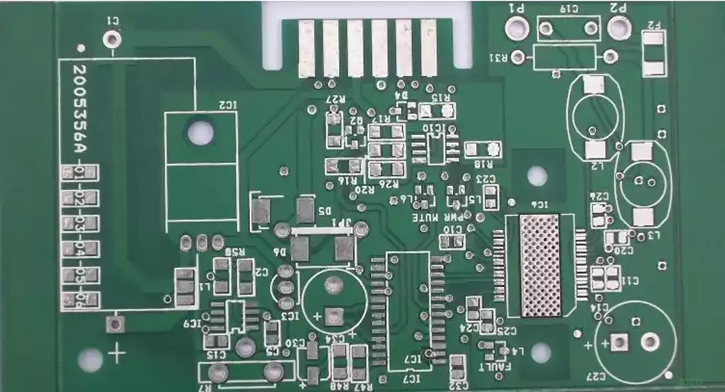
Dry film pcb is a photosensitive polymer film, usually composed of polyester support film, photoresist layer and protective film. In the PCB manufacturing process, through the exposure and development steps, the dry film can form a precise conductive pattern. Dry film is an important consumable for making dry film PCB and is widely used in the microelectronics industry and circuit board manufacturing industry.
Dry film is relative to wet film. Dry film is a polymer material. It can produce a polymerization reaction after being irradiated by ultraviolet light to form a stable substance attached to the board surface, thereby achieving the function of blocking electroplating and etching [3].
Advantages of dry film
- It has a higher resolution, and the general line width can be 3-4mil; Wet film has higher resolution, but when making precision circuits, it is easy to get stuck due to its thin film.
- Dry film is used in graphic electroplating process. Electroplating thickening is carried out between high and vertical walls. When the coating thickness is less than the resist thickness, it can prevent coating protrusion and prevent resist from embedding under the coating when removing the film, ensuring line accuracy;
- The thickness and composition of dry film are consistent, avoiding discontinuity during imaging and high reliability
- When making thick copper plates (greater than 2oz), there is a corresponding thickened film, which is easy to make
- It can seal holes, with a maximum sealing of 6.0. Reducing the process greatly simplifies the PCB manufacturing process, which is conducive to mechanization and automation
The film is thicker and not easy to rub during the transfer process
Dry film disadvantages - Relative to wet film, the cost is higher, and the cost ratio of wet film to dry film of equal area is about 1:7
- The uniformity of dry film lamination is not as good as wet film, and it is easy to wrinkle
- The rework cost is higher than wet film
Advantages of wet film: - The coating thickness of wet film is thinner (generally 0.3mil –0.5mil, while the dry film thickness is generally 1.2 mil to 1.5mil), the cost per square meter of wet film is reduced by 35%-50%
- The etching speed is faster than dry film, and the etching factor is better than dry film. After exposure, it does not need to be parked for direct development and etching, and can be directly connected to the line for processing
- The packaging cost of wet film finished products is reduced by 75%, and the cost of developer and stripper is reduced by 70%
- The cost of sewage and waste treatment is reduced by 30%
- When using wet film, the film and the film layer are directly attached during exposure, shortening the optical path, reducing light energy loss, and improving the accuracy of graphic transfer:
- As an anti-etching graphic, since the wet film is liquid and has leveling properties, it can eliminate the disconnection caused by scratches and pits, and the adhesion of the wet film is also improved, and it can avoid plating and reduce gaps.
Roll coating or other coating methods can be used, which is simple to operate, the degree of automation is improved, and the output is also increased accordingly.
Disadvantages of wet film:
- Since there is no protective film on the surface, the film is thin, and excessive manual operation is prone to scratches
- Too many stacked boards after rolling will cause sticking boards
- After rolling, the pinch point is easy to drop ink spots, causing dirt to stick to the film and forming positioning defects
4.Due to the evaporation of solvents during processing, good ventilation conditions are required, and harmful substances gather in the air, affecting the health of operators
- Compared with dry film, it is impossible to seal holes. For boards with or without copper holes, it is necessary to add two drills or plug glue particles to complete it
- Because the wet film coating is too thin, it is difficult to make thick copper plates (greater than Zoz)
- Drying is required, and the process time increases
- When making fine circuits (less than 4mil), it is easy to produce film sandwiches
9.The exposure energy is higher than that of dry film, and the exposure capacity is lower than that of dry film
The difference between the inner layer dry film and the outer layer dry film
- Different functional positioning:
The inner layer dry film is mainly used for the image transfer of the inner layer, which defines the circuit and plane of the inner conductive layer.
The outer dry film is used for the outer layer, directly covering the copper foil to form the final circuit pattern.
- Differences in performance requirements:
The inner dry film needs to have good adhesion and filling ability, because it is covered on the inner core board, and these locations may have uneven or rough surfaces.
The outer dry film pays more attention to resolution and line width control, because it is directly related to the conductive accuracy and appearance quality of the final product. - Differences in processing flow:
After imaging, the inner dry film usually needs to undergo multiple chemical processing steps such as etching and stripping to prepare for connection with the outer layer.
After imaging, the outer dry film may require additional electroplating processes in addition to development to increase the conductive performance. - The material composition may be different:
Due to its relatively harsh working environment, the inner dry film may require stronger alkali resistance and heat resistance.
The outer dry film may pay more attention to photosensitivity and resolution to ensure the accurate transfer of fine patterns.
https://ipcb.co/pcb/Understanding the difference between the inner and outer dry films is of great significance for optimizing PCB design and improving production efficiency. Different application requirements and process flows determine the differences in material selection, performance requirements and processing methods between the two. High-quality dry film PCBs can not only improve the performance of the circuit, but also ensure long-term stability and reliability.
Printed circuit manufacturers all hope to use dry films with good performance to ensure the quality of dry film pcbs, stabilize production and improve efficiency. In recent years, with the rapid development of the electronics industry, the precision density of printed circuit boards has been continuously improved. In order to meet the needs of printed circuit board production, new dry film products have been continuously launched, and the performance and quality have been greatly improved and improved.
When the dry film is applied, the polyethylene protective film is first peeled off from the dry film, and then the dry film resist is pasted on the copper clad board under heating and pressure. The resist layer in the dry film becomes soft after heating, and the fluidity increases. The film is applied with the help of the pressure of the hot press roller and the action of the binder in the resist. Film application is usually completed on a film application machine. There are many types of film application machines, but the basic structure is roughly the same. Generally, the film can be applied continuously or in a single sheet.
When laminating continuously, attention should be paid to aligning the dry film on the upper and lower dry film feed rollers. Generally, the size of the film should be slightly smaller than the board surface to prevent the anti-corrosive agent from sticking to the hot pressing roller. Continuous laminating has high production efficiency and is suitable for mass production. The three factors to be mastered when laminating are pressure, temperature, and conveying speed. Pressure: For a newly installed laminating machine, first adjust the upper and lower hot pressing rollers to be parallel to the axis, and then gradually increase the pressure to adjust the pressure. According to the thickness of the printed board, adjust it to make the dry film easy to paste, stick firmly, and wrinkle-free. Generally, the pressure can be fixed and used after it is adjusted. If the thickness of the circuit board produced is too different, it needs to be adjusted. The general line pressure is 0.5-0.6 kg/cm. Temperature: It varies slightly according to the type, performance, ambient temperature and humidity of the dry film. If the film is coated relatively dry and the ambient temperature is low and the humidity is low, the laminating temperature should be higher, otherwise it can be lower. A good and stable environment in the darkroom and intact equipment are good guarantees for laminating.
Generally, if the film temperature is too high, the dry film image will become brittle, resulting in poor plating resistance. If the film temperature is too low, the dry film will not adhere firmly to the copper surface. During the development or electroplating process, the film is prone to warping or even falling off. The film temperature is usually controlled at around 100°C. Conveying speed: related to the film temperature. When the temperature is high, the conveying speed can be faster. When the temperature is low, the conveying speed will be slowed down. The conveying speed is usually 0.9-1.8 m/min.
In order to adapt to the production of printed circuit boards with fine conductors, a wet film process has been developed. This process uses a special film machine to form a layer of water film on the surface of the copper foil before the dry film is applied. The function of the water film is to: improve the fluidity of the dry film; remove bubbles trapped in scratches, sand holes, pits and fabric depressions; during the heating and pressurizing film process, water has a viscosity-enhancing effect on the photoresist, thereby greatly improving the adhesion between the dry film and the substrate, thereby improving the qualified rate of fine conductors. It is reported that the qualified rate of fine conductors can be increased by 1-9% using this process.
Photosensitivity includes photosensitivity, exposure time tolerance and depth exposure. Photosensitivity refers to the amount of light energy required for the photoresist to undergo a polymerization reaction under ultraviolet light to form a polymer with a certain corrosion resistance. When the light source intensity and lamp distance are fixed, the photosensitivity is expressed as the length of the exposure time. A short exposure time means a fast photosensitivity. In order to improve production efficiency and ensure the accuracy of printed boards, a dry film with a fast photosensitivity should be selected.
After the dry film is exposed for a period of time, the photoresist layer has been fully or mostly polymerized after development. Generally speaking, the image formed can be used. This time is called the minimum exposure time. The exposure time is further extended to make the photoresist polymerize more thoroughly, and the image size obtained after development is still consistent with the image size of the base plate. This time is called the maximum exposure time. Usually, the best exposure time for the dry film is selected between the minimum exposure time and the maximum exposure time. The ratio of the maximum exposure time to the minimum exposure time is called the exposure time tolerance.
The depth exposure of the dry film is very important. During exposure, the light energy is reduced due to passing through the resist layer and the scattering effect. If the light transmittance of the resist layer is not good, when the resist layer is thick, if the exposure of the upper layer is appropriate, the lower layer may not react. The edge of the resist layer is not neat after development, which will affect the accuracy and resolution of the image. In severe cases, the resist layer is prone to warping and falling off. In order to polymerize the lower layer, the exposure must be increased, and the upper layer may be overexposed.
Dry film may become brittle due to the volatilization of solvents during storage, or may produce thermal polymerization due to the influence of ambient temperature, or uneven thickness due to local flow of resist, which is called cold flow. These seriously affect the use of dry film. Therefore, it is very important to store dry film in a good environment. Dry film PCBs should be stored in a cool and clean room to prevent storage with chemicals and radioactive substances. Storage conditions are: yellow light area, temperature below 27℃ (5-21℃ is best), relative humidity of about 50%. The storage period is no more than six months from the date of shipment, and those that pass the inspection beyond the storage period can still be used. During storage and transportation, moisture, heat, mechanical damage and direct sunlight should be avoided.
In order to avoid missed exposure and re-exposure during production operations, the color of the dry film pcb should change significantly before and after exposure, which is the color change performance of the dry film. When used as a mask for etching, the dry film is required to have sufficient flexibility to withstand the impact of liquid pressure during the development process and etching process without breaking, which is the masking performance of the dry film.
Whether it is the inner or outer layer of dry film, they are an indispensable part of the PCB manufacturing process, and their reasonable selection and use are directly related to the quality of the final product. With the continuous advancement of electronic technology, the requirements for dry film pcb technology will continue to increase, promoting the further development of material science and manufacturing technology.
