Introduction and Background
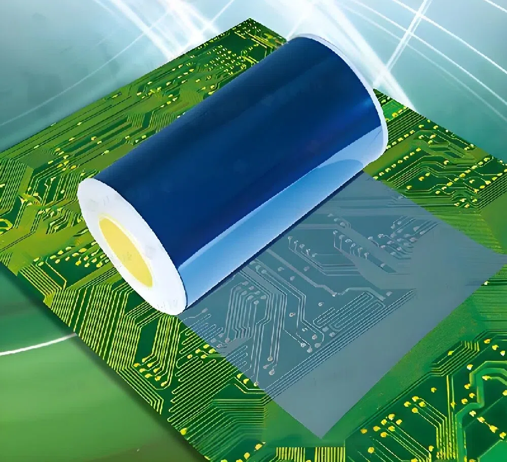
In the printed circuit board (PCB) manufacturing process, solder mask is a crucial step. It’s more than just a protective coating; it’s a key factor affecting soldering quality, circuit reliability, and overall circuit performance. The primary function of the solder mask is to cover the copper foil surface, protecting the circuit from oxidation, moisture, or short circuit failure during subsequent soldering or use. Among the many solder masking methods, dry film solder mask is a widely used process, particularly suitable for the production of high-precision, high-density, and high-reliability circuits.
Traditional liquid photoimageable solder mask (LPI) has been used in industry for many years, offering a mature process and reasonable cost. However, in certain specialized applications, its coverage, pattern refinement, and durability struggle to meet high-end requirements. In contrast, dry film solder mask, with its uniform thickness control, excellent resolution, and good chemical resistance, offers unique advantages in fine circuits, high-density interconnects (HDI), and specialized process circuits.
From a technological perspective, dry film solder mask isn’t a completely new invention. Instead, it has gradually matured and gained widespread application as the electronics industry pursued precision, reliability, and long-term stability. Its origins and development stem from the evolution of photolithography, which incorporated certain technical concepts from semiconductor manufacturing into PCB manufacturing. This has transformed PCB solder mask into more than just a protective layer; it has become a core process capable of high-precision pattern transfer and functional protection.
With the development of 5G communications, automotive electronics, medical electronics, aerospace, and high-speed computers, circuit boards are placing higher demands on the performance of solder mask materials. For example, the tiny pitch between BGA pads requires extremely high solder mask window precision, and the automotive and aerospace industries demand solder mask stability even in extreme environments. Consequently, dry film solder mask, with its unique performance, has become an increasingly discussed and adopted option among manufacturers and customers.
How Dry Film Solder Mask Works
To understand the value of dry film solder mask, it’s important to first understand how it works. Dry film solder mask is a photoresist material. Its core concept is to transfer patterns through a photosensitivity reaction, thereby forming a precise solder mask layer on the copper foil surface of the PCB.
Dry Film Composition
Dry film solder mask typically consists of three layers:
Polymer matrix layer: This is the main component of the dry film and determines the physical properties of the solder mask, such as toughness, adhesion, and heat resistance.
Photosensitive layer: Contains photoinitiators and monomers, which undergo cross-linking or polymerization under UV light, hardening to form a stable protective layer.
Protective film: This layer is primarily used to protect the photosensitive layer during storage and lamination to prevent contamination or premature reaction.
This structure ensures that the dry film has sufficient mechanical strength before transfer to the PCB surface, while also enabling the formation of high-resolution patterns after exposure and development.
Pattern Transfer Principle
The dry film solder mask process is similar to photolithography:
Lamination: The dry film is evenly applied to the PCB copper surface using a vacuum or heat press to ensure a bubble-free and wrinkle-free coating.
Exposure: UV light is selectively applied to the dry film surface using a mask (film). Cross-linking occurs in the exposed areas, hardening them into a solid solder mask layer, while unexposed areas remain soluble.
Development: An alkaline developer dissolves away the unexposed areas, leaving a precise solder mask pattern. The pads or vias are exposed, while the remaining areas are covered and protected.
Curing: Further curing is performed by heating or secondary UV exposure, imparting excellent chemical and heat resistance to the solder mask.
Through this process, dry film solder mask can create very clear solder mask openings at fine pitches, making it suitable for high-density packages such as BGAs and CSPs.
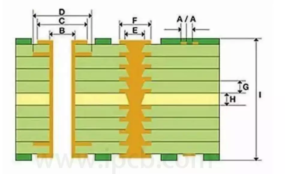
Differences from Liquid Solder Mask:
Liquid photoresist (LPI) is applied by screen printing or spraying, followed by exposure and development. The key difference between dry film solder mask and liquid solder mask lies in the pre-film morphology. Liquid solder mask is susceptible to uneven coating thickness or bubbles due to factors such as surface tension and copper surface topography during application. Dry film solder mask, on the other hand, achieves a more uniform thickness through lamination, making it particularly suitable for ultra-fine-pitch traces and pads.
Furthermore, because dry film solder mask is a thin film, it has sharper edges after development, resulting in higher resolution pattern transfer. Liquid solder mask, on the other hand, can exhibit blurred edges. This difference gives dry film solder mask an advantage in applications requiring micron-level precision.
Key Process Control Points
The effectiveness of dry film solder mask depends on several key steps in the process:
Lamination temperature and pressure: These directly impact the adhesion of the dry film to the PCB surface. Too low a temperature can lead to poor adhesion, while too high a temperature can cause premature cross-linking.
Exposure energy: This determines the extent of the photosensitivity reaction. Insufficient energy results in incomplete curing, while excessive energy can cause pattern distortion.
Development time and solution concentration: These must be strictly controlled to prevent underdevelopment (film residue) or overdevelopment (pattern erosion).
Curing process: Post-curing ensures the long-term reliability of the solder mask layer, including its heat resistance, chemical resistance, and mechanical strength.
Precise control of these steps can truly maximize the performance advantages of dry film solder mask.
Detailed Process Flow
The dry film solder mask process essentially involves precisely laminating a pre-formed photosensitive film onto a copper surface. The desired window pattern is then created through photolithography, and finally cured to form a long-term protective layer. The entire process can be broken down into several key steps: substrate pretreatment → lamination → alignment and exposure → development → cleaning and post-curing → inspection and rework. The following sections provide detailed process information, key control points, and common issues for each step.
Substrate Surface Preparation
Before lamination, the PCB surface must be thoroughly cleaned and activated to ensure good adhesion between the film and the copper surface. Common steps include degreasing, microetching (microetching), rinsing with clean water, and drying.
Purpose and Necessity: Removes oil, flux residue, oxide layers, and particles. Microetching increases surface roughness, enhances mechanical adhesion, and improves adhesion.
Typical Process: Alkaline degreasing → Acid microetching (light degreasing/etching) → Ultrapure water rinsing → Hot air or vacuum drying.
Key Control Points: Water washing should not leave water spots; micro-etching time and concentration must be determined based on the material (copper thickness, substrate type). Over-etching will affect circuit accuracy, while under-etching can cause delamination.
Common Defects and Solutions: If localized delamination or bubbles occur after lamination, this is likely due to insufficient pre-treatment or residual oil on the board surface. Rework, re-cleaning, and replacement of severely contaminated boards are required.
Lamination/Lamination
Laminating the dry film to the board surface is the most critical step in the dry film lamination process. Vacuum hot pressing lamination is commonly used to ensure bubble-free, uniform film layers, and perfect adhesion.
Method: Vacuum lamination or hot press roller lamination; first remove one side of the protective liner (depending on the process), apply the dry film to the copper surface, and then securely bond through heat and pressure.
Typical parameters (reference range): Lamination temperature is typically approximately 80–120°C (depending on the film type and substrate), lamination pressure is in the range of 0.1–0.6 MPa (1–6 bar), and speed and time must be adjusted to match the board and film thickness.
Critical Control Points: 1) Adequate vacuum to prevent bubbles; 2) A uniform temperature profile to avoid local overheating that may cause premature crosslinking of the film; 3) Cooling to room temperature after lamination before stripping.
Suitability: For flexible boards or thick copper boards, lamination parameters should be adjusted downward or a special adhesive layer should be used to prevent warping or film cracking.
Common Defects: Bubbles, wrinkles, partial lamination, and edge lift—mostly caused by improper lamination temperature/pressure or surface contamination.
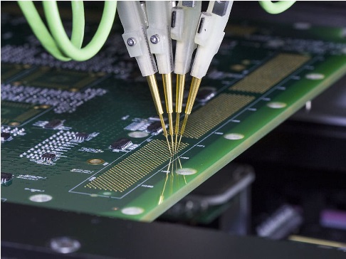
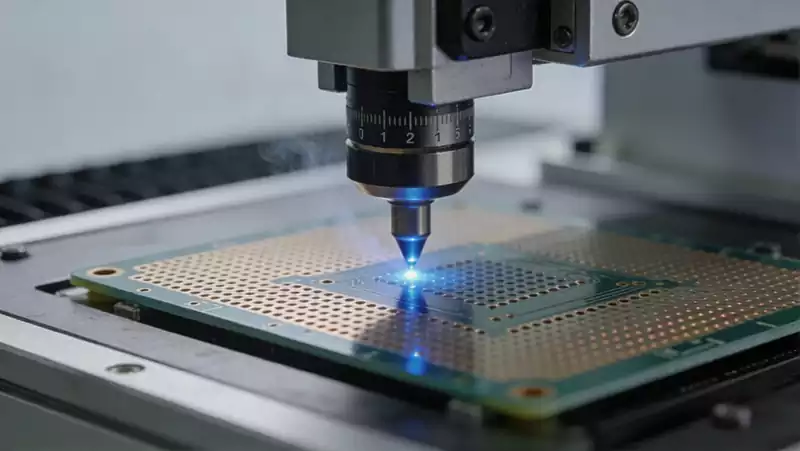
Alignment & Exposure
Exposure accuracy directly determines the geometric accuracy of the solder mask opening. After mask alignment, the dry film is exposed to UV light to cure the photosensitive areas.
Alignment Method: Optical alignment (fiducial positioning) or mechanical alignment. HDI and fine-pitch designs require extremely high alignment accuracy (micron-level).
Exposure Parameters: Exposure energy/dose, light source wavelength and uniformity, and exposure time are all critical. Typical exposure wavelengths are UV (near 365nm), and the exposure energy is adjusted according to the film manufacturer’s recommendations (exposure energy varies significantly between different film types).
Key Control Points: Ensure uniform light intensity to avoid overexposure at the edges or underexposure at the center; alignment errors must be controlled within design tolerances.
Defects and Prevention: Underexposure can result in residual film (solder mask residue), while overexposure can cause pattern expansion or bridging. Alignment deviation can cause pad window misalignment, affecting soldering reliability.
Development
Development involves dissolving and removing the unexposed (uncrosslinked) dry film, exposing the pads and the copper surface to be exposed. Alkaline developer is typically used for development.
Development Method: Spray or immersion development, using appropriate temperature and power (spray pressure or agitation).
Control Parameters: Developer concentration, temperature, and time require strict control. Excessively long or intense development can cause window size reduction or edge erosion, while too short a development period can result in film residue.
Cleaning Tips: After development, thoroughly rinse away any residual solution, ensure developer residue is removed, and dry the film to prevent any impact on subsequent curing or surface treatment.
Common Defects: Film residue (causing cold solder joints), overdevelopment (reduced window size or depressions), streaks, or discontinuities—mostly caused by improper development parameters or developer contamination.
Post-Curing (Post-Bake / Curing)
After development, the film requires a secondary curing step to achieve complete crosslinking and achieve the desired mechanical and chemical resistance. Post-curing is typically accomplished via thermal or UV curing.
Purpose: To improve the film’s heat resistance, chemical resistance, and mechanical strength to withstand processes such as reflow and wave soldering.
Curing Conditions: The curing temperature and time are specified by the film supplier. A secondary heat treatment at 90–150°C is common, lasting from tens of minutes to several hours, or a secondary UV exposure can be used to achieve partial crosslinking.
Note: The curing temperature must not exceed the upper tolerance limits of the substrate or film; the curing profile must match the reflow profile (ensuring it withstands the peak temperature of lead-free reflow, typically requiring a short peak of approximately 260°C).
Common Problems: Undercuring leads to poor temperature or chemical resistance; overcuring can make the film brittle, affecting bending reliability (particularly important for flexible applications).
Inspection, Repair, and Rework
After curing, the film enters the inspection stage. Qualified candidates proceed to subsequent surface treatment or assembly. Inspection includes visual, dimensional, electrical, and reliability testing.
Appearance Inspection: Automated Optical Inspection (AOI) is used to check for defects such as window location, edge definition, bubbles, and pinholes. AOI can quickly screen high-density boards.
Electrical and functional testing: Ensure that the solder mask does not contaminate the pad surface, causing poor contact. If necessary, perform a soldering test (test soldering) to verify solderability.
Mechanical testing: Peel/adhesion testing (according to IPC or factory standards) confirms that the film layer meets the required adhesion to the copper surface.
Reliability testing: Environmental testing such as thermal cycling, humidity and heat, and salt spray is used to verify long-term reliability, particularly for automotive and aerospace products.
Repair process: Minor defects discovered by AOI can be repaired using microspraying or localized redevelopment/recuring. Severe defects require rework or scrapping. Clear process specifications must be followed for repairs to avoid subsequent reliability issues.
Compatibility with Subsequent Processes
The dry film layer must be compatible with subsequent processes, such as surface treatment (ENIG, immersion tin), silk screen printing, SMT, and reflow soldering.
Surface treatment sequence: Different factories have different processes. Some surface treatments (such as ENIG) can be completed after solder mask application. The key is to ensure that the copper surface within the solder mask opening is clean and free of organic residue before surface treatment.
Reflow Compatibility: The film must withstand the peak temperatures of lead-free reflow without peeling, blistering, or color change. Selecting a film material that can withstand high temperatures and strictly controlling the curing profile are key.
Assembly and Testing: The solder mask must ensure reliable soldering to the pads and not fall off during functional testing, compromising contact.
Key Quality Control Points (KPCs) and Process Capability
To ensure stable mass production, key control points should be established and monitored:
Incoming Material Inspection: Dry film batch consistency (film thickness, photosensitivity profile, temperature resistance rating) and substrate quality (cleanliness, copper thickness, surface roughness).
Statistical Control of Lamination Parameters: Temperature, pressure, speed, and vacuum level must be recorded and SPC-controlled.
Exposure Dose and Development Time Control: Regularly calibrate the exposure system and development tank with test pieces to ensure pattern consistency.
In-Line Inspection: Automated Optical Inspection (AOI), peel testing, and regular environmental aging tests constitute quality barriers.
Common Defects, Causes, and Possible Solutions (Summary)
Bubbles or delamination: Commonly caused by surface contamination or insufficient vacuum before lamination; solutions include enhanced cleaning, increased vacuum, and adjustment of lamination parameters.
Development scumming: Insufficient exposure or development; solutions include increasing the exposure dose, extending the development time, or replacing the developer.
Window size deviation/bridging: Overexposure or misalignment; solutions include calibrating the exposure dose, improving alignment, and checking mask accuracy.
Delamination: Insufficient pretreatment or improper curing; solutions include re-optimizing the cleaning, micro-etching, and curing procedures, and performing adhesion testing.
Pinholes/microcracks: Defects in the film itself or damage to the lamination machinery; solutions include replacing the film batch, optimizing lamination roller/knife adjustments, and strengthening inspection.
Application Value and Industry Trends of Dry Film Solder Mask
In the printed circuit board industry, as products evolve towards higher density, higher reliability, and greater multifunctionality, traditional liquid solder mask materials are gradually becoming less effective, and dry film solder mask is increasingly being used in more manufacturing processes. Dry film solder mask’s continued success in this competitive market stems primarily from its unique performance advantages and wide adaptability.
First, in the consumer electronics sector, particularly in miniaturized products like smartphones, wearables, and tablets, PCB wiring density continues to rise. Traditional solder mask processes often struggle to maintain high-precision spacing control. Dry film solder mask, with its uniform coating and photoimaging process, maintains excellent coverage and stability in fine-pitch designs, thus preventing defects such as solder bridges and solder bridging. This makes it a preferred choice for many high-end electronics foundries.
Second, in the automotive electronics and new energy sectors, circuit boards must not only withstand long-term temperature cycling and mechanical stress, but also withstand the effects of oil, moisture, and corrosive media.Film solder mask demonstrates superior reliability and durability in these demanding operating conditions, and has become a growing trend in new energy vehicle power modules, charging station control units, and on-board radar systems. Compared to liquid solder mask, dry film’s heat resistance and mechanical strength provide longer product lifecycles and lower maintenance costs.
In high-frequency, high-speed circuit design, the dielectric properties of solder mask material directly impact signal transmission quality. Because dry film thickness and uniformity are easily controlled, its dielectric constant distribution is more stable, positively impacting impedance control for high-speed signals. This characteristic has led to the increasing adoption of dry film solder mask in applications such as RF communications, 5G base stations, and satellite antenna systems. It not only improves signal integrity but also provides designers with more predictable parameters for system-level optimization.
From an industry perspective, with increasingly stringent green environmental regulations, manufacturers must reduce solvent use and hazardous gas emissions. Dry film solder mask technology, by reducing chemical volatilization and cleaning steps, offers improved environmental compatibility and complies with regulations such as RoHS and REACH. Furthermore, in terms of production efficiency, the introduction of automated exposure and development technologies has made dry film solder mask more cost-competitive in large-scale production.
In the future, dry film solder mask is expected to continue to develop in the following three directions: First, material suppliers will continuously improve formulations to enhance its compatibility with new substrates such as flexible and rigid-flex boards; second, the combination of thick film and dry film processes may expand its application in power electronics; and third, with the introduction of artificial intelligence and automated inspection technologies, the yield and consistency of dry film solder mask processing will be further improved, better meeting the electronics manufacturing industry’s dual demands for high performance and low cost.
It can be said that dry film solder mask is not only a key process in current PCB manufacturing but also a key support for the future of high-end manufacturing towards precision, environmental friendliness, and reliability.
Comparison and Challenges of Dry Film Solder Mask and Traditional Solder Mask Processes
In the printed circuit board industry, the choice of solder mask process directly determines the reliability and production efficiency of the final product. Dry film solder mask and traditional liquid solder mask ink processes each have their own advantages and disadvantages. Therefore, manufacturers need to make appropriate trade-offs based on their product needs in different application scenarios.
Process Differences
Traditional liquid solder mask is typically applied evenly to the board surface via screen printing, spraying, or coating, followed by exposure and development to form a pattern. This method requires less equipment and offers more cost-effective materials. However, because the printing thickness is affected by the screen or coating process, it often suffers from uneven thickness and poor edge resolution. In contrast, dry film solder mask is applied to the PCB surface via a lamination process and pattern transfer is achieved using photolithography. This significantly improves resolution and thickness consistency, offering greater process advantages in high-precision circuit design.
Comparison of Refinement
Liquid solder mask can meet most requirements in general applications, but its defect rate increases significantly when the wiring pitch is below 100μm. Dry film solder mask achieves resolution levels unattainable with liquid processes, effectively preventing solder bridges, cold joints, and short circuits. Therefore, dry film solder mask has a more prominent application value in high-density interconnect (HDI) and advanced packaging processes such as BGA and CSP.
Environmental Adaptability and Reliability
Dry film solder mask generally performs better in terms of long-term heat resistance and mechanical strength. Due to its dense film layer and high surface flatness, it not only remains stable during high-temperature soldering but also provides excellent protection in harsh environments such as humidity and high salt spray. Liquid solder mask has relatively limited reliability under these conditions and is more suitable for consumer electronics or low-cost products with relatively moderate performance requirements.
Cost and Capacity Considerations
Liquid solder mask still has advantages in terms of material cost, especially in high-volume, low-precision production lines, where the overall cost-effectiveness of the liquid process is superior. While dry film solder mask offers superior performance, the material price and initial process equipment investment are higher. Furthermore, the lamination and photolithography steps are more complex, resulting in higher overall production costs. This investment is necessary for manufacturers pursuing high yield and high precision; however, for price-sensitive markets, the liquid process still has viability.
Current Challenges
Although dry film solder mask has seen rapid growth in the high-end market, its widespread adoption still faces several key challenges:
Material compatibility: The bonding performance of some flexible boards, thick copper boards, or special substrates is less stable than with traditional processes, requiring further improvement.
Process complexity: Compared to liquid processes, dry film processes require higher requirements for equipment precision, cleanroom environments, and operational standards, raising the manufacturing barrier.
Cost pressure: In mid- and low-end applications, customers are more focused on cost control, which has limited the widespread adoption of dry film solder mask.
Overall, dry film solder mask and traditional liquid solder mask are not simply substitutes, but rather complementary. Liquid solder mask continues to dominate the mid- and low-end, high-volume market, while dry film solder mask demonstrates unparalleled advantages in high precision, high reliability, and high added value. With continuous advancements in material technology and equipment processes, the distinction between the two may gradually blur, but it is foreseeable that the market share of dry film solder mask will continue to grow.
Material Selection and Process Optimization Recommendations
In dry film solder mask applications, material selection and process optimization directly determine the quality and cost control of the final product. Many manufacturers have found in actual production that even with advanced dry film processes, inappropriate materials or inadequate process parameter control can still lead to open circuits, short circuits, and reduced reliability. Therefore, the appropriate selection of solder mask materials and process optimization are key to promoting the stable development of this technology.
Key Points for Solder Mask Material Selection
Currently, there are a wide variety of dry film solder mask materials on the market, with manufacturers varying in thickness, flexibility, heat resistance, and development speed. Companies should focus on the following aspects when selecting:
Thermal stability: Maintaining resistance to delamination and cracking during high-temperature processes such as multiple reflow and wave soldering.
Adhesion: Secure adhesion to the copper foil and substrate surface to prevent subsequent delamination.
Resolution capability: Support for smaller pads and narrower pitch designs.
Chemical resistance: Maintaining stable performance in environments with acidic and alkaline solutions, flux, and cleaning fluids. For high-end products requiring long-term reliability, it is recommended to prioritize materials from internationally renowned manufacturers to ensure consistency and traceability. For cost-sensitive products, cost-effective domestic materials can be selected, but incoming material inspection should be strengthened to avoid process fluctuations caused by batch differences.
Key Process Control Steps
Lamination Step: The lamination process determines the quality of the dry film’s adhesion to the board surface. Strictly control the lamination temperature and pressure to ensure the film is free of bubbles and wrinkles.
Exposure Step: Exposure energy and alignment accuracy directly impact the transfer of pattern quality. High-precision equipment and a stable light source are key to ensuring resolution.
Development Step: Balance the developer concentration and spray pressure to avoid over- or under-development, which can lead to solder mask defects.
Curing Step: The curing temperature and time must strictly follow the material manufacturer’s recommendations. Under-curing can result in reduced reliability, while over-curing can affect the film’s flexibility.
Common Process Optimization Methods
In practice, many companies adjust the dry film solder mask process based on the specific characteristics of individual customer projects. For example:
For high-density interconnect (HDI) boards, reducing film thickness improves precision, but simultaneously optimizing exposure parameters is necessary to prevent film cracking.
For thick copper or high-power boards, increasing film thickness appropriately enhances insulation and voltage resistance.
During the small-batch pilot production phase, a gradual adjustment approach is employed, documenting yield performance under different parameters to establish an optimal process window.
Collaboration with the Supply Chain
Optimizing the solder mask process is not solely a manufacturing task; it also requires close collaboration with material suppliers and equipment manufacturers. For example, material manufacturers often provide detailed application manuals and test data, while equipment manufacturers can provide targeted debugging recommendations. Only by integrating this information with their own production line conditions can manufacturers maximize the advantages of dry film solder mask.
Future Optimization Directions
Future material research and development will focus on higher resolution, lower thermal expansion coefficients, and improved environmental performance. At the same time, with the development of intelligent manufacturing, automated and digital process control methods will become increasingly prevalent. For example, by monitoring light intensity and developer concentration in real time and automatically adjusting parameters, manufacturers can reduce human error and improve consistency.
In summary, material selection and process optimization for dry film solder mask are not simply improvements in a single process, but rather a systematic project involving design, materials, equipment, and process control. Only through the coordinated efforts of these multiple aspects can the goals of high yield and high reliability be truly achieved.
Summary
In modern PCB manufacturing, dry film solder mask has become a key technology supporting the production of high-precision, high-reliability circuit boards. It not only offers excellent resolution and consistency, meeting the demands of increasingly compact designs, but also excels in heat resistance, chemical resistance, and environmental performance. Through appropriate material selection, rigorous process control, and close collaboration with the supply chain, manufacturers can improve production efficiency and reduce costs while ensuring product quality.
With the continuous development of the electronics industry, especially the rise of 5G, automotive electronics, and high-performance computing, the application of dry film solder mask will further expand, and materials and processes will continue to be optimized. It can be foreseen that this technology will continue to play an irreplaceable role in promoting PCB manufacturing towards higher precision, higher reliability and greater environmental protection.