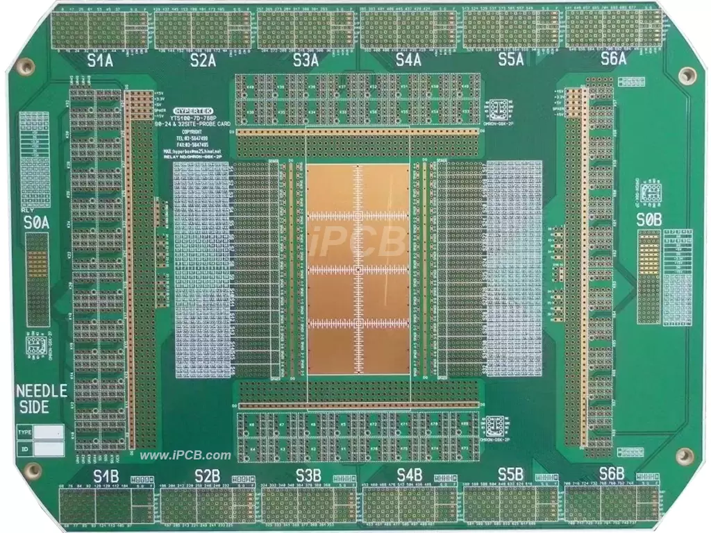
Electrical Contact Pad is a conductive area on a PCB (Printed Circuit Board) used to connect electronic component pins or wires. The pad is usually made of copper and is plated (such as tin or gold) to enhance its conductivity and corrosion resistance. The quality and design of electrical contact pads are critical to PCB performance and reliability.
Type of electrical contact pad
According to different uses and manufacturing processes, pads can be divided into the following types:
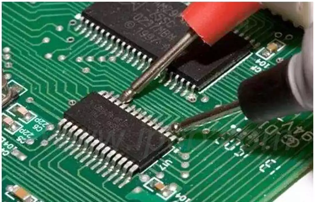
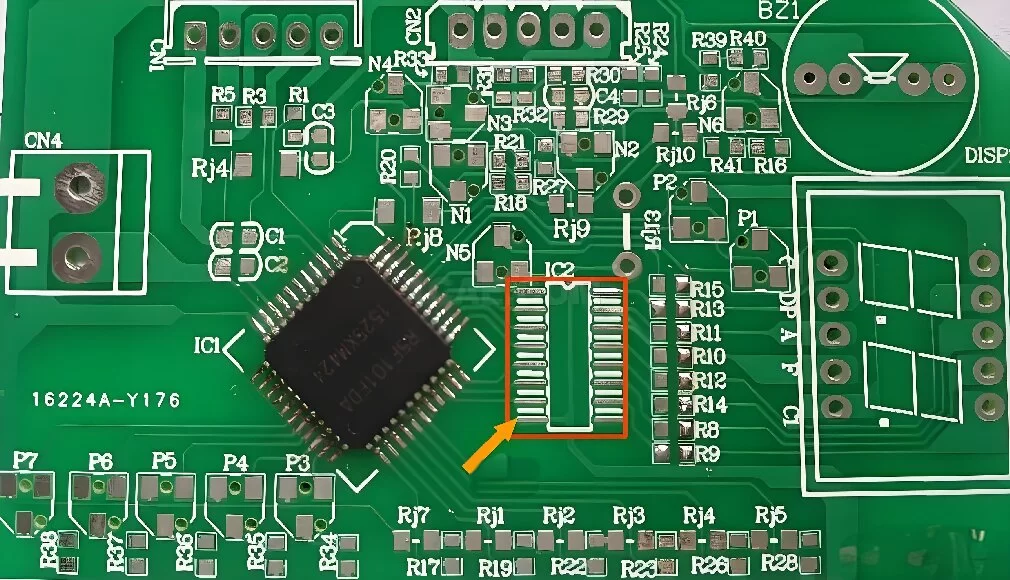
1. Pin pad: Pin pad refers to the metal contact point where pin components are soldered on the PCB. The pin pad usually consists of a circular or oval metal ring, and the pin can be directly inserted into the metal ring for soldering.
2. Surface mount pad: Surface mount pad refers to the metal contact point of electronic components soldered on the PCB surface through SMT (Surface Mount Technology). The surface mount pad is usually a flat metal pad used to connect the solder pins of SMT components.
3. Through-hole pad: Through-hole pad refers to the metal contact point on the surface and inner layer of the PCB. It is usually used for soldering pin components or connecting inner circuits. The through-hole pad consists of a metal ring and a conductive hole.
Pad design and fabrication
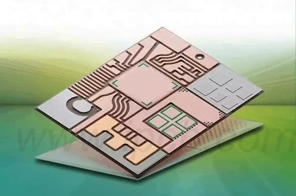
The design and manufacturing of the pads have an important impact on the performance and stability of the PCB. When designing pads, you need to consider the following factors:
1. The shape and size of the soldering pad: The shape and size of the soldering pad need to match the soldering feet of the component to ensure the stability and firmness of the soldering.
2. Welding pad layout: The welding pad layout needs to consider the size, quantity and location of components to ensure welding reliability and overall performance.
3. Material of the soldering pad: The material of the soldering pad needs to have good conductivity, corrosion resistance and heat resistance to ensure the quality and stability of the welding.
When manufacturing pads, a copper pouring process is usually used. The copper coating process refers to covering a layer of copper foil on the surface or inner layer of the PCB, and then forming the pad through chemical etching and mechanical processing. The manufacturing of pads requires highly precise processes and equipment to ensure the quality and stability of the pads.
Pad maintenance and repair
When using PCB, the pads may be damaged due to service life, mechanical damage, electrical failure, etc. In order to ensure the normal operation of the PCB, the pads need to be maintained and repaired.
When maintaining pads, the connectivity and stability of the pads need to be checked regularly. If the pad is loose, detached or damaged, it needs to be repaired or replaced in time.
When repairing pads, professional welding equipment and tools need to be used to ensure the quality and stability of the pads. When welding, you need to pay attention to the welding temperature, time and welding position to avoid poor welding or damage to electronic components.
Quality Control of Electrical Contact Pads
Visual inspection: Examine the surface quality and shape of the pads through a microscope.
Electrical testing: Ensure pad conductivity and reliability.
Environmental testing: performance testing that simulates actual usage environments.
Electrical contact pad applications
Consumer electronics: such as applications in smartphones, tablets and home appliances.
Industrial Control: Used in industrial automation and control equipment.
Automotive electronics: Applications in automotive electronic control units (ECUs).
Summarize
The solder pad is a metal contact point on the PCB used for soldering components and is a very important component of electronic products. The design and manufacturing of the pads have an important impact on the performance and stability of the PCB. When using PCB, the pads need to be maintained and repaired to ensure the normal operation of the PCB.
Electrical contact pads play a vital role in the design and manufacturing of PCBs, influencing their functionality and durability. As technology advances, innovations in pad design and materials continue to enhance PCB performance, paving the way for more sophisticated electronic devices.