ELIC PCB (Every Layer Interconnect PCB) is a high-end PCB (Printed Circuit Board) type, also known as any-order or any-layer HDI (High Density Interconnect) PCB.
Subtractive ELIC (Arbitrary Layer) interconnect is a PCB fabrication technique that is part of the subtractive method, whereby unwanted metal is removed to form a circuit pattern. This technique is common in the production of high-end HDI PCBs for boards with high density and high interconnectivity. Subtractive ELIC (Every Layer Interconnect) technology allows connections to be made between each layer of the board,enabling an arbitrary layer plating process, which is accomplished through stacked copper-filled microvias that pass through each layer of the board,allowing designers to create a pattern of circuits in the PCB by removing unwanted metal. Enables designers to establish a connection between any two layers in the PCB after stacking to maximize interconnect density. This technology increases the level of flexibility, allowing designers to utilize board space more efficiently while supporting high-end technologies, including IC carrier boards.
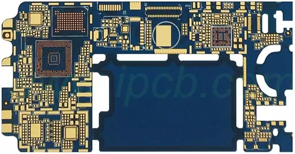
HDI pcb is mainly categorized into first-order, second-order, third-order, and Anylayer HDI, with gradually shrinking feature sizes and increasing manufacturing difficulties. Currently, the main boards used in electronic terminal products are third-order,fourth-order,or Anylayer HDI. Anylayer HDI is known as any-order or any-layer HDI main boards, or ELIC (Every Layer Interconnect) HDI, and the main boards used in electronic terminal products are 10 or 12 layers.
The characteristics of arbitrary order HDI circuit boards (elic pcb) mainly include high density, high reliability, high performance and good reproducibility.
High density: HDI circuit boards are able to realize high-density wiring and connections in a limited space, thanks to its sophisticated manufacturing process and high-quality materials, so that the performance and efficiency of electronic equipment has been significantly improved.
High Reliability:Thanks to its precision manufacturing process and high-quality materials,HDI circuit boards have high reliability and stability,and can meet the performance requirements of modern electronic products.
High performance:HDI circuit boards support high-speed data transfer and low-power operation,which is critical for modern electronic systems that require high-frequency operation and fast data transfer.
Good Repeatability:HDI circuit boards have high design flexibility and can be customized according to different needs,with good repeatability to ensure product consistency and reliability.
In addition, HDI circuit boards offer unparalleled stability and efficiency through advanced design and technology, providing more connection options through microvia technology, optimizing power distribution and ground layout,and Reducing noise and electromagnetic interference ensures pure and stable current.
During the manufacturing process,HDI boards utilize stringent quality control measures,including the use of high-quality materials,fine processing techniques, and exhaustive testing procedures to ensure that performance is maintained even under harsh operating performance is maintained even under harsh operating conditions.
Stacking impedance is a very important parameter in PCB design.
It directly affects the quality of signal transmission.Therefore,there are some specific design techniques that need to be followed when designing ten-layer HDI (1st order, 2nd order, 3rd order, 4th order, any order) stacked layer impedance.
First, we need to choose the right material.Generally speaking, using materials with low dielectric constants can reduce the stacking impedance.
In addition, we need to consider factors such as the thickness and coefficient of thermal expansion of the material.
Secondly,we need to lay out the copper foil reasonably.
In the design process,we should try to avoid copper foils that are too long or too short.In addition,attention should be paid to the spacing between copper foils to ensure the stability of signal transmission.
Third, we need to control the direction of the line.In the design process,we should try to avoid lines that are too zigzag or cross.In addition,attention should also be paid to the distance between the lines to prevent signal interference.
ELIC pcb is usually manufactured using a sequential lamination process,which involves bonding multiple layers of material together using heat and pressure.
Lamination (PRESSING) is the process of bonding the layers of wiring together with the aid of a B-order semi-cured sheet.This bonding is achieved by mutual diffusion and penetration of macromolecules at the interface,which in turn creates intertwining.The purpose is to press the discrete multilayer boards together with the bonding sheets into multilayer boards of the desired number of layers and thickness.
The stacked boards are fed into a vacuum hot press. Using the heat provided by the machine, the resin inside the resin sheet is melted to bond the substrate and fill in the gaps.
For designers, the first thing to consider with lamination is symmetry.This is because the board is subjected to pressure and temperature during the lamination process, and there will be stresses in the board after the lamination is complete.Therefore,if the laminated board is not uniform on both sides, the stress is not the same on both sides, causing the board to bend to one side, greatly affecting the performance of the circuit board.
In addition,even in the same plane,if the distribution of copper cloth is not uniform,will cause the resin flow rate is not the same at all points, so that the thickness of the cloth copper less places will be slightly thinner, while more copper cloth thickness will be slightly thicker places. In order to avoid these problems, in the design of the cloth copper uniformity, the symmetry of the stack, blind buried hole design layout and so on all aspects of the factors must be carried out in detail rate.
Elic pcb high multi-order arbitrary board manufacturing difficulties and challenges
- material production difficulty. HDI board structure is more complex than ordinary boards, the requirements of the material performance is also higher. In addition to the strict requirements of the material ZTE,sometimes it is necessary to use some difficult to process materials,such as PTFE,PPO,PI and so on. The processing of these materials is prone to thermal stress,rise and fall and other problems, which have a great impact on the difficulty of making the board.
- inter-layer connection difficulty.HDI design,line layers,connection points are concentrated, if all connections are perforated connection, will inevitably lead to too high a frequency of perforation,affecting line stability and board performance.At this time the need to use blind and buried hole technology.But buried holes are difficult and expensive;blind holes need to rely on laser drilling, fixed-depth drilling and other high-precision equipment for processing,but also prone to poor perforation quality and other issues.
- Difficulty of blind hole production. Blind hole production technology requirements are higher,because the perforation can not be repaired,once the quality is unqualified, it is necessary to make a new board.HDI board blind hole production requires three steps:drilling,then interface activation,and finally copper plating. Among them, the drilling precision requirements are particularly high.
- line precision. Elic pcb line width line spacing is also difficult to produce. elic pcb board layers,the line is getting more and more fine, for the location of the line, thickness, bending angle, etc. There are strict requirements, line precision will affect the electrical performance of the board. Many manufacturers need to be equipped with micro-precision processing equipment, such as laser cutting machine,laser laser engraving machine, etc., in order to ensure that the line in the high-precision range of production.
ELIC PCB, as a high-end PCB technology, shows important application value in the electronic manufacturing industry through its arbitrary layer interconnection characteristics. It solves the problem of high-density, high-reliability circuit board manufacturing and provides strong support for the performance improvement of electronic products.