What is EMI? EMI is short for Electromagnetic Interference, which usually refers to the phenomenon of interference with neighboring electronic products when electronic products are in operation.
EMI is a problem that occurs when a source of interference in an electronic system couples with a receiver (i.e., some component of the electronic system.) EMI can be categorized according to its coupling medium: conducted or radiated.
Conducted EMI (low frequency, 450 kHz to 30 MHz)
Conducted EMI is coupled to pcb components by conduction through parasitic impedance as well as power and ground connections. Noise is transmitted to another device or circuit by conduction.Conducted EMI can be further divided into common mode noise and differential mode noise.
Common mode noise is conducted through parasitic capacitance and high dV/dt (C × dV/dt).It is transmitted through the parasitic capacitance along the path of any signal (positive or negative) to GND
Differential mode noise is conducted through parasitic inductance (magnetic coupling) and high di/dt (L × di/dt).
Radiated EMI (high frequency, 30 MHz to 1 GHz)
Radiated EMI is noise that is transmitted wirelessly to the device to be tested via magnetic field energy.In switching power supplies,this noise is the result of high di/dt coupled with parasitic inductance. Radiated noise affects neighboring devices.
Hazards of EMI?
The seriousness of EMI hazards can be seen from the relevant certifications developed and enforced by various national organizations. First of all, EMI will affect the performance of electronic terminal equipment, serious will lead to its inability to work properly.EMI into the power grid, will cause serious harmonic pollution, on the grid other electrical appliances caused by interference.
The high voltage breakdown or burnout of electronic and electrical equipment caused by EMI, and the resulting serious damage to the surrounding items, can bring about huge economic losses or casualties.EMI can also cause some harm to the human body.
In order to avoid the impact of EMI on electronic equipment, you can start from the following aspects:
- Reasonable layout and design of electronic equipment: In the design and layout of electronic equipment, electromagnetic radiation and coupling effects should be minimized. For example, sensitive components and sources of interference can be separated, and appropriate shielding measures.
- Selection of low EMI electronic components: selection of low EMI electronic components can effectively reduce the radiation and sensitivity of electronic equipment. For example, you can choose low-noise amplifiers,low inductance coils and low capacitance inductors and other components.
- Increase filters: filters can effectively inhibit the propagation of EMI.Adding appropriate filters in the circuit can reduce the propagation of EMI and interference.
- Grounding and shielding:Grounding and shielding are two commonly used methods to reduce EMI. By connecting the ground of the electronic equipment to a low-impedance grounding pole, the noise current on the ground can be reduced;and the use of appropriate shielding materials for electronic equipment shielding can reduce the propagation of electromagnetic waves and interference.
- Software filtering:For some highly sensitive electronic equipment, you can use software filtering methods to reduce the impact of EMI. By filtering the signal in the software, you can effectively reduce the noise and interference.
EMC and electromagnetic energy generation, propagation and reception are closely related to the PCB design do not want to appear EMC. electromagnetic energy from multiple sources, they are mixed together, so special care must be taken to ensure that different circuits, alignments, apertures and PCB materials to work together, a variety of signals are compatible and do not interfere with each other.
Electromagnetic Compatibility (EMC), refers to the ability of devices and systems to interact with each other,generate electromagnetic interference and exhibit good coexistence.EMC is very important to ensure the stability,reliability and interoperability of electronic equipment.
The Three Elements of Electromagnetic Compatibility
EMC consists of three elements: electromagnetic field tolerance (EFT),electromagnetic radiation resistance (EMS) and ground disturbance (GND). These elements address a variety of EMI issues for electrical equipment and systems and are considered from the design stage.
The first key element of EMC: Electrical Transient Withstand (EFT)
EFT focuses on the sudden voltage fluctuations and current pulses at the standard frequency of the power system, which are widely found in many electrical devices and systems. The key to ensuring the stable operation of these devices and avoiding failures caused by external disturbances is to manage and control these transient electromagnetic disturbances.
The second core element of EMC: Electromagnetic Emission Suppression (EMS)
EMS focuses on reducing the amount of electromagnetic energy radiated into the surrounding space by equipment and systems during operation to prevent unwanted electromagnetic interference with neighboring environments or other equipment. Through careful design and application of electromagnetic compatibility (EMC) strategies, we can effectively reduce electromagnetic emissions and promote harmonious coexistence and functional compatibility between equipment.
The third major aspect of EMC: interference caused by the grounding system (GND)
Ground disturbance usually refers to the voltage and current crosstalk generated by the shared grounding path. Through the adoption of scientific grounding layout and measures, can significantly reduce or even eliminate the electromagnetic interference problems caused by such shared grounding, and thus protect the overall electromagnetic compatibility and stability of the system.
Tips to avoid electromagnetic problems in PCB design
Tip1:Ground the PCB
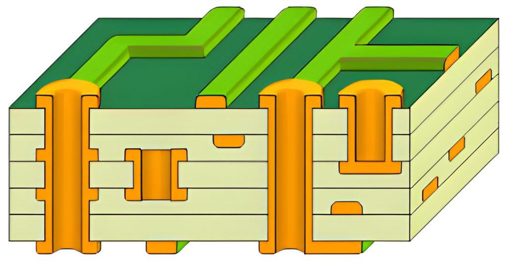
An important way to reduce EMI is to design the PCB grounding layer. The first step is to make the grounding area as large as possible within the total PCB board area, which will reduce emissions, crosstalk and noise. Special care must be taken when connecting each component to a ground point or grounding layer; if this is not done, the neutralizing effect of a reliable grounding layer cannot be fully utilized.
A particularly complex PCB design has several stabilized voltages. Ideally, each reference voltage has its own corresponding ground plane. However, too many grounding layers would increase the manufacturing cost of the PCB and make it overpriced. A compromise is to use separate grounding layers at three to five different locations, each of which can contain multiple grounding sections. This not only controls the manufacturing cost of the board, but also reduces EMI and EMC.
Low impedance grounding systems are important if EMC is to be minimized. In a multi-layer PCB, it is better to have a reliable grounding layer rather than a copper balancing block (copper thieving) or loose grounding layer because it has a low impedance, provides a current path, and is the best source of reverse signals.
The length of time for the signal to return to ground is also very important. The time the signal spends traveling to/from the source must be comparable, or an antenna-like phenomenon will occur, making the radiated energy part of the EMI. Similarly, the alignment for transferring current to/from the signal source should be as short as possible; if the source and return paths are not equal in length, ground bounce will occur, which also generates EMI.
Tip2: Crosstalk and alignment are key points
Alignment is especially important to ensure proper current flow. If the current is coming from an oscillator or other similar device, it is especially important to keep the current separate from the grounding layer, or to keep the current from running in parallel with another alignment. Two parallel high-speed signals can generate EMC and EMI, especially crosstalk. It is important to keep the resistor path as short as possible and the return current path as short as possible. The return path alignment should be the same length as the send alignment.
For EMI, one is called the “violating path” and the other the “victim path”. Inductive and capacitive coupling affects the “victimized” alignment due to the presence of electromagnetic fields, which generate forward and reverse currents on the “victimized alignment”. This creates ripple in a stable environment where the length of the signal being sent is almost equal to the length of the signal being received.
In a well-balanced environment with a stable alignment, the induced currents should cancel each other out, eliminating crosstalk. However, we are in an imperfect world where this does not happen. Therefore, our goal must be to keep crosstalk to a minimum for all alignments. The effect of crosstalk can be minimized if the width between parallel lines is twice the width of the alignment. For example, if the alignment width is 5 mils, the minimum distance between two parallel lines should be 10 mils or greater.
PCB designers must also continue to deal with EMC and interference issues as new materials and components continue to emerge.
Tip 3: Distinguish between EMI
Since EMI is different, a good EMC design rule is to separate analog and digital circuits. Analog circuits have higher amperage or higher currents and should be kept away from high-speed alignments or switching signals. If possible, they should be protected with grounded signals. On multilayer PCBs, the analog traces should be routed on one ground plane and the switching traces or high-speed traces on another. Thus, signals with different characteristics are separated.
Sometimes a low-pass filter can be used to eliminate high-frequency noise that is coupled to the surrounding alignment. The filter suppresses the noise and returns a stable current. It is important to separate the ground layers of analog and digital signals. Since analog and digital circuits have their own unique characteristics, it is critical to keep them separate. Digital signals should have a digital ground and analog signals should terminate at an analog ground.
In digital circuit design, experienced PCB layout and design engineers pay special attention to high-speed signals and clocks. At high speeds, signals and clocks should be as short as possible and adjacent to the ground plane because, as mentioned earlier, the ground plane keeps crosstalk, noise, and radiation within manageable limits.
Digital signals should also be located away from the power plane. If they are very close, noise or inductance can occur, which can weaken the signal.
Tip 4: Optimize Decoupling Capacitor Layout to Suppress Crosstalk
Decoupling capacitors play a key role in electronic equipment, they are cleverly placed between the power pin and ground pin, designed to weaken the negative impact of crosstalk. By doing so, the AC impedance can be significantly reduced, thus effectively minimizing noise and signal interferences. In order to maintain a low impedance at different frequencies, it is recommended that multiple decoupling capacitors be used in combination.
When laying out decoupling capacitors, a crucial principle is to ensure that the capacitors with the smallest capacitance values are placed close to the device in order to minimize their contribution to the inductive effect of the alignment. This means that such capacitors should be placed directly adjacent to the power supply pins or power supply alignment and seamlessly connected to the via or grounding layer via pads for optimal electrical connection. If longer alignments are encountered, it is recommended to increase the number of via holes to further reduce ground impedance and optimize overall electrical performance.
Tip 5: Optimize Cabling Angles to Reduce EMI
In order to reduce electromagnetic interference (EMI), the wiring process should try to avoid the formation of 90-degree right angles between the alignment, vias and other electronic components, because this right-angle structure will exacerbate the generation of electromagnetic radiation. The right angle will gather additional capacitance, resulting in a sudden change in characteristic impedance, which in turn triggers the phenomenon of signal reflection, ultimately increasing the risk of EMI. To improve this, it is recommended to use at least two smooth transitions at 45-degree angles at cabling corners to reduce electromagnetic emissions and optimize the quality of signal transmission.
In the face of the challenge of emi, through the comprehensive use of selection strategies, we can effectively improve the anti-interference ability of electronic equipment to ensure its stable operation in the complex electromagnetic environment. As technology continues to advance, we look forward to more breakthroughs in the field of electromagnetic compatibility.