Definition and Function of Solder Mask Material in PCB Design
In the printed circuit board (PCB) manufacturing process, solder mask is a crucial protective coating. It’s typically green, hence the nickname “green board,” but PCBs can also come in red, blue, black, white, and other colors. The solder mask material not only impacts the board’s appearance but also profoundly influences its reliability, solderability, heat resistance, and long-term performance.
Solder mask is primarily applied to the copper foil surface, excluding the pads, to prevent solder bridging during soldering. It also provides insulation, moisture resistance, dust protection, and corrosion protection. With the miniaturization and higher density of electronic products, the performance requirements for solder mask are becoming increasingly stringent, especially in flexible printed circuits (FPCs), high-density printed circuit boards (HDIs), and high-frequency, high-speed boards. The material’s performance directly impacts the stability of the overall device.
Solder Mask Classification
Solder masks can be categorized into several types based on their composition, curing method, and application method. Common classifications include:
Photoimageable Solder Mask (PISM)
This forms a pattern through exposure and development, making it suitable for fine-line PCBs and the current mainstream application material.
Thermal Cure
This cures by heat and is commonly used in traditional processes, but lacks the precision of photosensitive solder masks.
Liquid vs. Dry Film
Liquid solder masks are more suitable for automated spray coating, while dry films are suitable for lamination processes for precision, high-density PCBs.
The physical properties, heat resistance, electrical performance, and adhesion of these solder mask materials all affect the overall quality of the finished board.
Composition and Performance Specifications of Solder Mask Materials
A high-quality solder mask material often requires a combination of performance advantages. Its composition and performance specifications are crucial to achieving excellent insulation, chemical resistance, thermal stability, and process compatibility.
Basic Components of Solder Masks
The composition of solder mask materials can be broadly categorized as follows:
Resin
Resin is the primary matrix of the solder mask, determining its structural strength and chemical stability. Commonly used resins include epoxy, polyimide, and acrylic. Epoxy resin is most widely used in rigid circuit boards due to its excellent adhesion and electrical properties. Polyimide is more suitable for flexible circuit boards due to its greater flexibility and high-temperature resistance.
Photoinitiators/Curing Agents
Photosensitive solder masks require photoinitiators, which promote a cross-linking reaction under ultraviolet light, thereby curing the material. Thermosetting solder masks use thermosetting agents to achieve the same effect.
Fillers
Inorganic fillers such as silica powder and alumina can enhance the solder mask’s wear resistance and thermal expansion resistance, while also adjusting its fluidity.
Solvents
A suitable amount of organic solvent (such as PGMEA and glycol ether) is used in liquid solder films to adjust viscosity and coating properties. These solvents evaporate completely after curing.
Additives
Such as leveling agents, anti-settling agents, colorants, and stabilizers are used to improve film formation and longevity.
Key Performance Indicators
To achieve excellent performance in actual PCB applications, solder film materials must generally meet the following key indicators:
Heat Resistance
The solder film must withstand the high temperatures of the soldering process, typically maintaining color, blistering, and peeling at 260°C.
Adhesion
Strong adhesion between the solder film and the copper foil and substrate is essential to prevent peeling and flaking caused by alternating hot and cold temperatures. Adhesion is often assessed using the cross-cut test.
Insulation Resistance
Ensures that leakage between different circuits due to moisture or contamination is prevented. This is particularly critical in high-frequency and high-voltage circuits.
Chemical Resistance
The solder film must resist corrosion from chemicals such as acidic and alkaline etching solutions, flux, and cleaning agents, without swelling or deterioration.
Process Compatibility
This includes screen printing compatibility, exposure clarity, development speed, and spray uniformity, which impact production yield.
Color Stability
The color should be uniform and not change dramatically over time or temperature, especially in applications where branding demands high aesthetics.
CTI (Comparative Tracking Index)
Indicates the material surface’s ability to withstand arcing. A higher CTI indicates a better insulation rating.
A high-quality solder film material must not only meet basic performance standards but also demonstrate enhanced stability, reliability, and environmental friendliness to meet the complex demands of modern electronics manufacturing.
Application Differences and Selection Recommendations for Solder Film Materials
As electronic products evolve toward higher frequencies, higher speeds, thinner weights, and greater functionality, PCB types are becoming increasingly diverse, ranging from traditional rigid and flexible boards to high-frequency and high-speed boards, metal substrates, and high-density dielectric boards. Different types of PCBs have varying performance requirements for solder mask materials. Therefore, in actual production, it’s crucial to select the appropriate solder mask material based on the PCB type and end-use scenario.
Rigid PCBs
Rigid PCBs are the most common type of PCB, used in computers, communications, home appliances, and other fields.
Recommended solder mask material features:
Primarily based on an epoxy resin system, offering high cost-effectiveness;
Excellent heat resistance and adhesion;
Compatible with conventional hot air leveling (HASL) and lead-free HASL surface finishes;
Strong process adaptability, suitable for high-volume automated production.
Selection Recommendations:
A medium-viscosity, single-component heat-curing solder mask can meet the requirements of traditional PCB manufacturing processes.
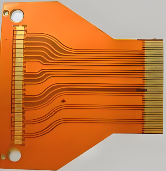
Flexible Printed Circuits (FPCs)
Flexible printed circuits are used in lightweight, compact applications such as wearable devices, mobile phone camera modules, and medical devices.
Recommended Solder Mask Material Features:
Polyimide or modified acrylic-based systems offer excellent flexibility;
Thin film dry film coverlay or liquid curable material;
Maintains excellent adhesion and insulation after repeated flexing;
High heat resistance, resists warping or cracking.
Selection Recommendations:
It is recommended to use low-stress, fold-resistant solder masks developed specifically for flexible circuit boards, and pay attention to compatibility with the adhesive system.
High-frequency/High-speed PCBs
These boards are widely used in applications such as 5G communications, automotive radar, RF microwaves, and servers, requiring extremely high signal integrity.
Recommended Solder Mask Material Features:
Extremely low dielectric constant (Dk) and dissipation factor (Df);
Excellent flatness to prevent uneven signal propagation paths;
Precisely controlled thin coating thickness to avoid impedance shift caused by excessive thickness;
High reliability, maintaining insulation and adhesion after repeated thermal shocks.
Selection Recommendations:
Preferably choose photosensitive liquid solder films optimized for surface adhesion to high-speed materials (such as PTFE and LCP) to avoid delamination or peeling due to incompatibility.
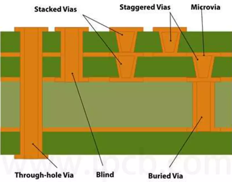
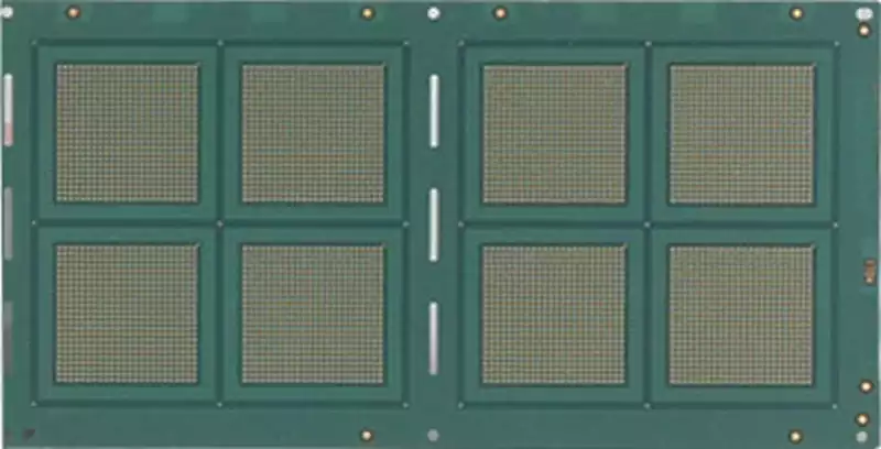
HDI (High-Density Interconnect) Boards
HDI boards feature high integration and wiring density and are widely used in miniaturized end products such as smartphones and tablets.
Recommended Solder Film Material Features:
High-resolution development performance, suitable for intricate graphic designs;
Extremely thin coating capability, avoiding masking of fine lines;
Highly reliable surface coverage, preventing CAF and ion migration;
Excellent compatibility with HDI processes such as laser drilling and plasma processing.
Selection Recommendations:
It is recommended to use high-precision photosensitive solder films in conjunction with advanced process equipment such as automated exposure and development.
Metal Substrates (such as aluminum substrates)
Metal substrates are often used in applications with high heat dissipation requirements, such as LED lighting and power devices.
Recommended solder mask material features:
Excellent thermal stability, withstanding short-term temperatures above 300°C;
Strong adhesion, preventing peeling during thermal cycling;
Excellent heat dissipation, without hindering heat conduction;
Compatible with spray coating, dip coating, and other processes.
Selection Recommendations:
High-temperature epoxy solder masks designed for metal substrates can be used. In some cases, a white, high-reflectivity solder mask may be used to enhance LED light efficiency.
In summary, solder mask materials are not a “one-size-fits-all” option; instead, they should be precisely matched to the specific PCB type, end-use application requirements, and production process conditions to achieve a balance between performance, reliability, and cost.
Testing and Quality Control of Solder Mask Materials
Solder mask materials must not only meet the basic process requirements of printed circuit board manufacturing but also undergo a series of rigorous tests to ensure their reliability and stability in practical applications. This section will discuss standard testing methods and common quality control measures to provide a deeper understanding of the performance evaluation mechanisms of solder mask materials.
Standard Test Items
During the PCB manufacturing process, solder mask ink testing is typically conducted according to international standards (such as IPC-SM-840). Tests include, but are not limited to, the following:
Adhesion Test: Using the cross-hatch test, a grid pattern of cuts is made on the solder mask surface, followed by affixing tape and then removing it to assess ink adhesion strength.
Hardness Test: Using a pencil hardness test or a niobium needle scratch test to test the ink’s post-curing hardness, the solder mask is typically required to meet certain friction and scratch resistance requirements.
Thermal Shock Test: The sample is alternately immersed in high and low temperatures (e.g., -65°C and +125°C) to observe for cracking, peeling, and other signs of delamination.
Solvent Resistance Test: Using common cleaning agents such as isopropyl alcohol and rosin flux, the ink’s resistance to solvents is tested to prevent dissolution or blistering during subsequent manufacturing processes.
Insulation Resistance Test: Confirms that the solder mask maintains excellent insulation properties even in humid environments, preventing potential hazards such as short circuits and leakage.
Solder Heat Resistance Testing: By simulating thermal shock environments such as wave soldering and reflow soldering, the solder mask layer is observed for peeling, discoloration, or cracking.
These tests effectively ensure the stability and reliability of solder mask materials in diverse manufacturing environments and usage scenarios.
Quality Control Measures
To maximize the performance of solder mask materials, manufacturers must implement strict quality control measures in actual operations:
Raw Material Batch Control: Different batches of ink should be individually documented and tested with incoming material inspection to ensure traceability of each batch.
Ink Stirring and Usage Time Control: Most solder mask inks require thorough stirring before use and should be used within a specified timeframe to prevent poor printing due to viscosity fluctuations.
Screen Screen and Exposure Process Standardization: Proper selection of screen mesh, screen tension, and exposure energy helps ensure sharp edges and uniform thickness of the solder mask pattern.
Baking and Curing Parameter Monitoring: Temperature, time, and heating curve should be strictly controlled to prevent incomplete curing that could affect ink performance.
AOI and Visual Inspection: Automated Optical Inspection (AOI) is used to check for solder mask window accuracy and pattern offset, supplemented by manual visual inspection for verification.
Process Environment Cleanliness Management: Preventing interference factors such as dust, moisture, and static electricity from causing solder mask defects is particularly important in high-density printed circuit boards (HDI).
A series of systematic and standardized inspection and control measures can maximize the stability of solder mask material performance, reduce product failure and rework rates, and thus improve overall process yield.
Trends and Challenges of Solder Mask Materials in Future Electronic Applications
As the electronics industry continues to advance towards higher density, higher speed, miniaturization, and multifunctionality, solder mask materials are facing increasingly complex and demanding technical challenges. Traditional solder mask inks are gradually approaching their physical limits in terms of performance. Therefore, developing new, higher-performance solder mask materials is a key step in driving the PCB industry’s upgrade.
New Trend: High-Performance, Multifunctional Solder Mask Materials
Higher Thermal Stability
With the prevalence of high-power devices, PCBs are facing more frequent and severe thermal shocks. For example, control panels for new energy vehicles and high-frequency antenna modules for 5G base stations place new demands on the heat resistance of solder mask materials. Currently, some advanced green solder mask materials have achieved Tg values exceeding 150°C and can withstand short-term soldering temperature shocks exceeding 260°C.
Low Dielectric Constant and Low Loss
In high-frequency, high-speed circuits, the electrical performance of solder mask layers is crucial, especially in the millimeter-wave region, where even the slightest dielectric loss can compromise signal integrity. Developing solder mask formulations with low Dk and Df has become a key research focus for material suppliers.
Ultra-Thin and Compatible with Fine Patterns
In high-end applications such as HDI boards and IC substrates, controlling solder mask thickness is crucial. Too thick can lead to blurred copper outlines and uneven pads, while too thin can ineffectively cover the circuits, reducing insulation. Modern inks now support precise windowing of patterns below 20μm, enabling high-density design requirements when used with laser direct imaging (LDI) equipment.
Development of Environmentally Friendly Materials
RoHS and REACH regulations are driving the PCB industry towards halogen-free, low-VOC, and low-odor materials. Currently, green and environmentally friendly solder mask inks are gradually replacing traditional solvent-based products to reduce their impact on the environment and operator health.
Intelligent Compatibility and Functional Expansion
Some new solder mask materials have been endowed with additional functional properties, such as UV resistance, thermal conductivity, and even EMI shielding. These properties make them more than just a protective layer; they become an essential component of the circuit system.
Challenges
Despite the continuous emergence of new materials, the development of solder mask materials still faces several challenges:
Material Compatibility
Today, there are many different types of PCB substrates (such as PTFE, PPS, and BT resin). Each material has different adhesion requirements for solder mask inks, making a single formula difficult to adapt to all substrates and requiring case-by-case customization.
Compatibility with Advanced Process Equipment
With the increasing popularity of new processes such as LDI and inkjet printing, parameters such as particle size, viscosity, and exposure response speed of traditional solder mask inks need to be redesigned to meet the requirements of these new processes.
Balancing Performance and Cost
High-performance solder mask materials are often expensive. How to control material costs without sacrificing reliability is a challenge that material suppliers and PCB manufacturers must jointly address.
Narrowing Process Window
The processing window for high-end solder mask materials is relatively narrow, with stricter requirements for humidity, temperature, and stirring methods. Improper handling can significantly increase scrap rates and place higher demands on the technical skills of engineers.
Response Strategies and Future Outlook
Future solder mask materials will not only be a “protective layer” but also a “system integration layer.” To meet these challenges, the industry needs to work together in the following areas:
Material suppliers must strengthen cooperation with PCB manufacturers and end-brand customers.Collaborate with the industry to participate in pre-design evaluations and develop more targeted ink systems;
Promote the development of intelligent process platforms to achieve automated and parameterized management of ink application, exposure, and curing;
Introduce AI modeling to predict material stability under different conditions, accelerating the certification and iteration of new materials;
Continuously update industry standards to adapt to the quality requirements of new processes and materials, establishing an effective risk control system.
Driven by high-end applications in smart electronics, automotive electronics, aerospace, and other fields, solder mask materials will continue to play an irreplaceable role. Those who can first seize the three major trends of “functionality + reliability + greenness” are expected to lead the future market.