Definition and Development Background of HDI Flexible Circuit Boards
Driven by the trend toward increasingly thinner, smaller, and highly integrated electronic products, traditional rigid circuit boards are no longer able to meet the diverse product forms and complex circuit design requirements. In particular, in high-end sectors such as consumer electronics, medical devices, aerospace, and automotive electronics, increasingly stringent requirements for space utilization, signal integrity, and mechanical performance are driving the continuous evolution of new circuit board technologies. Among these, HDI flexible circuit boards (HDI Flex PCBs) have emerged as a high-end carrier that combines high-density interconnect (HDI) and flexible circuit technologies.
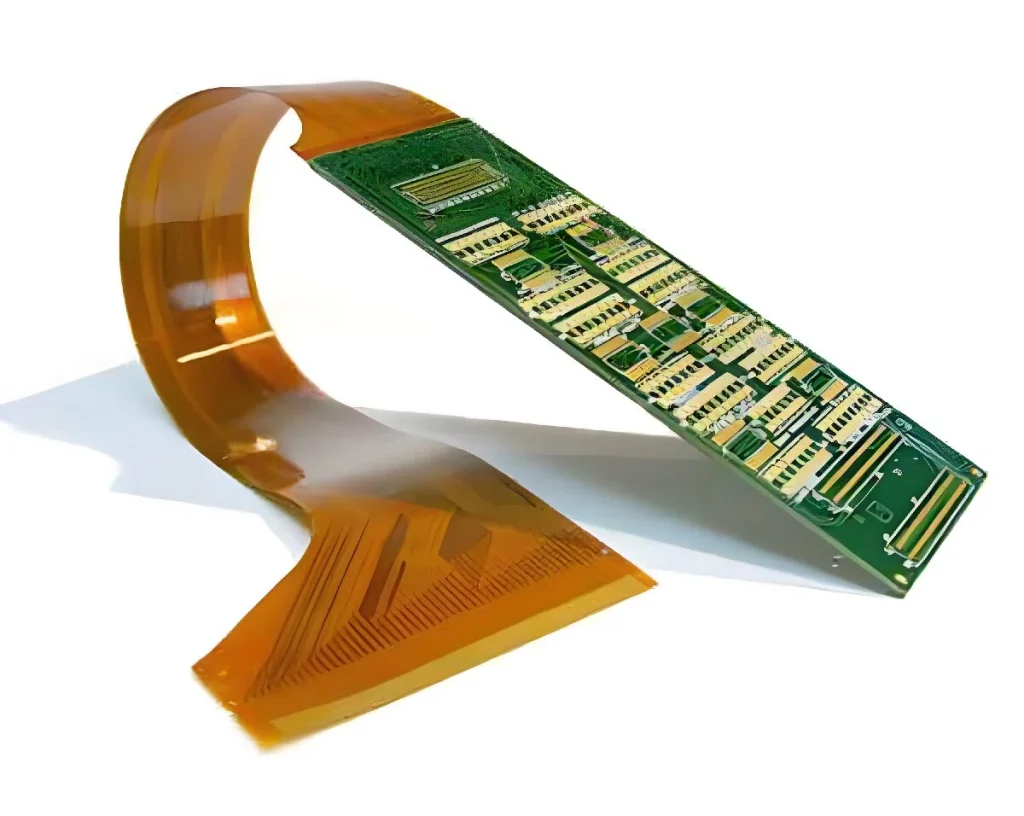
What is an HDI flexible circuit board?
HDI Flex PCBs utilize advanced laser drilling, fine-line etching, and buried and blind via processes on a flexible substrate (such as polyimide (PI)) to achieve high-density wiring and high-level interconnects. They not only possess the bendability and three-dimensional routing capabilities of flexible PCBs, but also offer the higher wiring density, smaller pads, narrower trace widths and spacing, and superior electrical performance of HDI boards.
In short, HDI flexible circuit boards have both “flexibility” and “high density” technical advantages, showing extremely high value in precision electronic applications.
Background of the integration of HDI and Flex PCB technology
Flexible circuit boards (Flexible PCB) originated in the 1960s and were originally used in the military and aviation fields. With its advantages of lightness, foldability, and space saving, it has gradually penetrated into various high-end electronic devices. HDI technology (High Density Interconnect) originated in the early 1990s and was first introduced by Motorola, IBM and other manufacturers to meet the needs of mobile communication products for miniaturization and high-speed signals.
As smart terminals, wearable devices, drones, medical imaging equipment, etc. put forward higher requirements for circuit board performance, the combination of HDI and FPC has become an inevitable trend. HDI Flex PCB realizes the synergy of two advanced PCB technologies, which not only meets the structural flexible space wiring, but also greatly improves the signal transmission efficiency and component packaging capabilities.
Application Scenarios in Current Industries
Currently, HDI flexible circuit boards are primarily used in the following applications:
The connection area between smartphone motherboards and camera modules
Microcircuit systems in wearable devices
Dynamic wiring in medical endoscopic imaging equipment
Weight-sensitive circuit design for aerospace instrumentation
High-density connections between central control consoles and sensor modules in high-end vehicles
All of these scenarios place stringent demands on PCB spatial structure, electrical performance, and mechanical toughness. The introduction of HDI Flex PCBs effectively addresses technical bottlenecks that traditional designs struggle to overcome.
Structural Characteristics of HDI Flexible Circuit Boards
HDI flexible circuit boards (HDI Flex PCBs) combine the advantages of high-density interconnects and flexible materials in their structural design, resulting in a far greater complexity than conventional FPCs (flexible printed circuit boards) or conventional HDI rigid boards. This section will delve into the core structural characteristics of HDI flexible boards, including their layer configuration, interconnection methods, material selection, and layout.
Layer Configuration and Structural Patterns
HDI flexible boards typically utilize a multilayer design to meet the demands of higher-density electronic connections within a smaller footprint. Common structures include:
Single- or double-sided flexible substrates with one or more HDI microvia layers.
Multi-level HDI structures (such as 1+N+1 and 2+N+2) increase wiring density through stepped interconnections.
Combined structures, such as rigid-flex PCBs, achieve high-density interconnections between the flexible and rigid regions using laser microvias.
This structure enables HDI flexible boards to accommodate complex chip layouts and multiple signal paths, making them particularly suitable for miniaturized, high-performance electronic products.
Microvia Technology
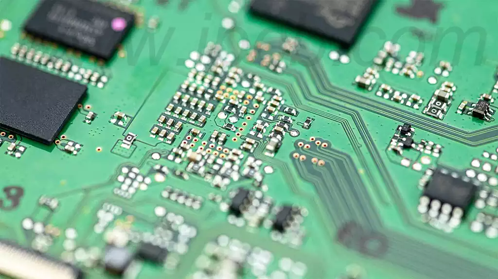
One of the key features of HDI boards is microvia technology. Flexible HDI also uses a laser drilling process to create blind vias with diameters of 50–75μm, connecting conductive paths between adjacent layers. Its features include:
Laser drilling enables smaller apertures and denser wiring;
Highly controllable laser processing area effectively avoids thermal damage to the flexible material;
Via filling technology further improves reliability and prevents voids during soldering. The ductility of flexible materials requires stricter control over laser drilling energy density, spot diameter, and processing time, making manufacturing more challenging than rigid boards.
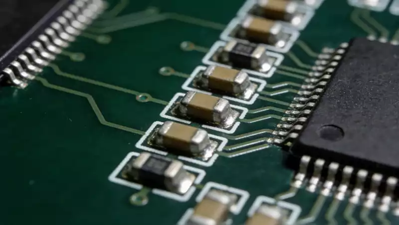
Conductive Material and Copper Foil Thickness Design
Common copper foil types for HDI flexible boards include rolled copper (RA copper) and electrolytic copper (ED copper). Rolled copper is more common in dynamic folding applications due to its superior ductility and crack resistance.
Thickness generally ranges from 12–35μm. Too thick can affect flexibility, while too thin can reduce current carrying capacity.
Surface treatments such as ENIG (electroless nickel gold) or OSP (organic solderability preservative) also affect signal integrity and soldering performance.
In HDI areas, to ensure soldering and reliability, localized thickened copper can be designed (localized thick copper technology).
PI Substrate and Adhesive Selection
Polyimide (PI) is the most commonly used insulating material in HDI flexible boards. Its advantages include high heat resistance, good flexibility, and excellent electrical properties. However, in HDI structures, substrate selection requires greater attention:
Low-flow adhesive (PI) is often used in multi-layer lamination to prevent adhesive overflow and affect blind via reliability;
Adhesive-free PI can reduce interlayer thickness and improve microvia yield;
Thin PI (e.g., 25μm) can accommodate smaller bend radii and higher wiring density requirements.
Multi-layer alignment and lamination processes
Because HDI flexible boards involve multiple lamination processes, interlayer alignment accuracy must be extremely high, often requiring the assistance of a CCD optical positioning system.
Alignment tolerances must be controlled within ±25μm;
The hot press temperature must be increased in stages to prevent interlayer shifting caused by thermal expansion and contraction of the flexible substrate;
Resin flow control must also be coordinated with microvia copper filling and copper thickness balance to prevent warping or deformation.
Detailed Explanation of the HDI Flex PCB Manufacturing Process
The manufacturing process for HDI flex PCBs (HDI Flex PCBs) combines high-density interconnect technology with the processing characteristics of flexible materials. Its process complexity is significantly higher than that of traditional rigid PCBs or conventional flexible PCBs. Below, we will detail the key manufacturing processes and core technology points.
Material Preparation
The base material of HDI flex PCBs is typically polyimide (PI) or other substrates with excellent flexibility, heat resistance, and electrical properties. These materials must exhibit high dimensional stability and excellent surface cleanliness to ensure the subsequent high-precision production of fine patterns and multi-level blind and buried vias.
In multi-layer designs, in addition to the flexible coverlay, pre-treatment and stackup planning of composite materials such as laser drilling films and adhesive layers may also be involved.
Pattern Transfer and Etching
Because HDI flex PCBs typically utilize extremely fine line widths and spacings (e.g., less than 50μm/50μm), the pattern transfer process requires the use of high-resolution dry film or liquid photoresist, combined with LDI (Laser Direct Imaging) equipment, to ensure pattern accuracy. The etching process requires extremely strict control over temperature, time, spray angle, and solution concentration; even the slightest deviation can result in missing circuits or short circuits.
Laser Drilling and Microvia Processing
One of the most critical processes in HDI flexible circuits is the production of microvias. Traditional mechanical drills cannot meet the processing requirements for diameters less than 100μm, so laser drilling is widely used, particularly a combination of CO₂ laser and UV laser processes.
CO₂ lasers are suitable for removing cover films and drilling through PI materials.
UV lasers are suitable for high-precision positioning and processing thin copper layers, avoiding ablation of the underlying material.
In addition, to ensure the integrity of the via walls and the quality of subsequent electroplating, laser vias often require plasma desmearing and activation.
Blind/Buried Via Plating and Filling Technology
The electroplating requirements for HDI flexible circuits are extremely stringent. Ensure that the copper filling inside the blind vias is uniform and void-free, otherwise reliability issues will occur. Current mainstream technologies include:
Electroless copper (Electroless Cu) + electroplating thickening
Via fill plating
Laminar thickening and controlled plating uniformity
This step typically utilizes horizontal plating lines and pulse plating techniques to improve hole filling and surface smoothness.
Lamination and stacking
For multi-level HDI flexible boards, multiple lamination processes and blind/buried via stacking are employed. Temperature control during the lamination process is crucial, especially for flexible materials, to prevent board warping or delamination. The film used for lamination must maintain good flowability and controllability to avoid affecting the flatness of the blind vias after copper filling.
Before lamination, each layer requires pattern alignment, pre-press baking, and cleaning to avoid the risk of open circuits caused by stacking offset.
Surface Treatment and External Protection
The surface treatment options for HDI flexible circuit boards vary depending on the customer’s application. Common options include:
OSP (Organic Solderability Preservative): Suitable for short-term use and products with high environmental requirements;
ENIG (Electroless Nickel Gold): Widely used for terminals requiring soldering reliability and corrosion resistance;
ENEPIG (Electroless Nickel Palladium Gold): Suitable for specialized applications such as high-frequency and wire bonding.
For external protection, Coverlay lamination is often used, or in some structures, Photoimageable Solder Resist (PSR) is used to create a patterned solder mask.
Electrical Testing and Visual Inspection
100% electrical testing is required at the end of the manufacturing process to detect opens and shorts. Automated Optical Inspection (AOI) visual inspection, cross-section testing, and thermal cycling testing are also performed to verify product reliability under various environments.
Key Points in HDI Flexible Circuit Board Structural Design
During the design of HDI flexible circuit boards (HDI Flex PCBs), the structural layout directly impacts reliability, manufacturing feasibility, and cost control. Compared to traditional rigid boards or standard FPCs, HDI flexible circuit boards require a high level of precision and meticulousness in their structural design due to their multi-layered design, microporous design, and optimized space and weight. The following details the stackup structure, blind and buried via design, transition between flexible and rigid areas, and trace and pad arrangement.
Stackup Structure Design
HDI flexible boards typically have no more than six layers, with 2-4 layers being the most common design. Due to flexibility requirements and manufacturing cost constraints, the greater the number of layers, the thicker the board, which in turn impacts flexibility. Therefore, the distribution of signal, power, and ground layers must be carefully planned from the beginning of the design process to ensure optimal functionality and a compact structure.
Core Layer Arrangement: It is recommended to place the ground or power layer close to the signal layer to create a stable impedance-controlled structure.
Symmetrical Design: Ensure symmetry in thickness and stress across the entire stackup to prevent warping or delamination during bending or reflow soldering.
Dielectric Material Selection: Highly flexible materials such as polyimide (PI) should be preferred, with thin copper layers or adhesive laminated between layers to ensure good adhesion.
Micro Blind and Buried Via Design
One of the core features of HDI is the use of laser-drilled micro blind vias (laser vias) and buried vias (buried vias). This technology helps achieve high-density routing, reduces interconnect space, and improves signal integrity.
Aperture Size Control: Laser blind vias typically have a diameter of 0.1–0.15mm and should be controlled within the material and process capabilities to avoid carbonization of the hole wall and a decrease in hole formation rate.
Stepped Blind Vias: Multiple stacked blind vias can be used to achieve higher-layer connections, but copper filling or prepreg filling is required to prevent plating defects.
Buried Via Layout: Generally used for mid-layer connections to avoid affecting the folding and torsional performance of the flexible zone.
Rigid-Flex Structure Design
Many HDI flexible circuit boards use a rigid-flex structure, combining rigid and flexible zones within a single board. This structure greatly optimizes space and wiring harnesses, but design considerations require stress relief and pad reliability in the rigid-flex transition zone.
Transition Zone Routing: Avoid right-angle turns in signal lines; prefer circular arc connections to reduce stress concentration.
Flexible Zone Reinforcement: Improve the tensile strength and flex life of the flexible zone by applying reinforcing ribs (such as PI reinforcement sheets) or stacking multiple layers of PI.
Rigid Zone Pad Design: Ensure adequate pad size, stable through-hole soldering, and avoid using large copper areas in the transition zone.
Tracing, Spacing, and Impedance Control
Because HDI flexible circuit boards are often used for high-speed or high-frequency signal transmission, trace width, spacing, and impedance matching are extremely stringent.
Minimum Line Width and Spacing: This should be tailored to the manufacturer’s capabilities, generally starting at 0.05mm/0.05mm, with some processes supporting up to 30μm.
Differential Line Routing: For high-speed signals, differential pair routing is recommended, with strict equal length and spacing between the two lines.
Impedance Control: Flexible materials have a low dielectric constant, so simulation software is required for predictive design to ensure impedance stability within ±10%.
Power and Ground Return Paths: It is recommended to plan the ground plane appropriately to reduce signal return path impedance and avoid signal interference.
Pad Design and SMT Compatibility: HDI flexible circuit boards are widely used in consumer electronics and medical devices and often require compatibility with high-density surface-mounted devices (SMD) components. Therefore, special attention must be paid to the design of the pads and SMD areas.
BGA Pad Design: Laser blind vias are used to connect from the surface layer to the inner layer to avoid through-holes and increase SMD component density.
SMT Area Reinforcement: It is recommended to use a localized reinforcement layer under the pad to improve solder joint strength and prevent cracking during bending.
Shielding Window: For pads under the flexible area, precise windowing and solder mask ink design should be used to ensure printing accuracy and solderability.
Summary: A Key Piece in the Development of Future Electronic Products
HDI flexible circuit boards (HDI Flex PCBs), with their superior electrical performance, extremely high wiring density, and exceptional mechanical flexibility, play an increasingly important role in today’s high-end electronic devices. They are ubiquitous in applications ranging from smart wearables, mobile communications, medical devices, to aerospace.
As end products evolve towards smaller, thinner, and more intelligent designs, the performance requirements for flexible HDI boards continue to rise. Manufacturing capabilities, design techniques, and material selection will all become important criteria for evaluating a supplier’s capabilities.
For buyers, selecting an HDI flex PCB manufacturer with high-precision process capabilities, strict quality control, and flexible customization capabilities will directly impact product performance and market competitiveness. For design engineers, a thorough understanding of HDI flex PCB structural design rules, lamination methods, and process limitations is a key prerequisite for achieving high-performance products.
HDI flex PCBs are not the future; they are already here. The sooner you understand and apply it, the more you will stand out from the competition.