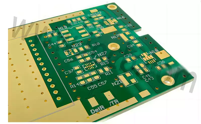
The manufacturing of microwave pcb has multiple distinctive features, primarily manifested in the diversity of substrate materials, stringent requirements for design precision, computer-controlled manufacturing processes, specialised graphic production, diverse surface coating options, CNC-controlled shape processing, and automated batch production inspection equipment.
Substrate Material Diversity
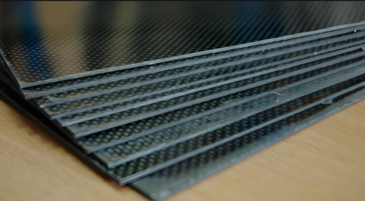
The miniaturisation and integration of microwave devices have imposed higher demands on the materials used in microwave PCB. Historically, domestic production has primarily relied on domestically produced glass cloth-reinforced polytetrafluoroethylene (PTFE) copper-clad laminates, but these materials are limited in variety and exhibit poor dielectric property uniformity, rendering them unsuitable for high-performance applications. Since the 1990s, microwave substrate materials from the RT/Duroid series and TIM series produced by American company Rogers have gradually been introduced for use. These materials include glass fibre-reinforced PTFE-clad copper boards, ceramic powder-filled PTFE-clad copper boards, and ceramic powder-filled thermosetting resin-clad copper boards. Despite their high cost, their superior dielectric and mechanical properties still offer significant advantages. Currently, such microwave substrates, particularly those with aluminium substrates, are being widely adopted. The variety of microwave printed circuit board substrates continues to increase, and design requirements are also rising, necessitating continuous optimisation of manufacturing processes to meet market demands.
Design Precision
The design of microwave pcb is evolving towards smaller size, lighter weight, higher reliability, and higher density interconnections, which urgently requires improvements in manufacturing processes, particularly in terms of high-precision manufacturing capabilities. The density requirements for microwave pcb design are continuously increasing. In the manufacturing of microwave printed circuit boards, the control of graphic dimension precision involves six aspects and ten parameters, including insulation layer thickness. High-frequency signal transmission imposes strict requirements on the characteristic impedance value of printed circuit boards, with typical line width/spacing tolerances of 0.02 mm, and even stricter tolerances of 0.015 mm. Defects in signal transmission lines, such as pits, serrations, notches, pinholes, and scratches, are not permitted, as these defects can impair signal transmission. The emergence of multi-layer microwave printed circuit boards has addressed the limitations of traditional single- and double-sided microwave pcb boards in meeting high-density and high-precision requirements, enabling high-density and high-precision signal transmission.
Computer-controlled
High-precision microwave PCB template design and manufacturing, CNC machining of shapes, and batch production inspection all rely on computer technology. The manufacturing of microwave PCB is moving towards computer-controlled processes. By integrating CAD with CAM and CAT technology, data processing and process intervention on CAD designs generate corresponding CNC machining files and inspection files for production process control and inspection. The enhanced processing capabilities of computer technology and increased information storage capacity urgently require high-speed signal transmission, making the extensive application of computer technology in microwave printed circuit board manufacturing an inevitable choice.
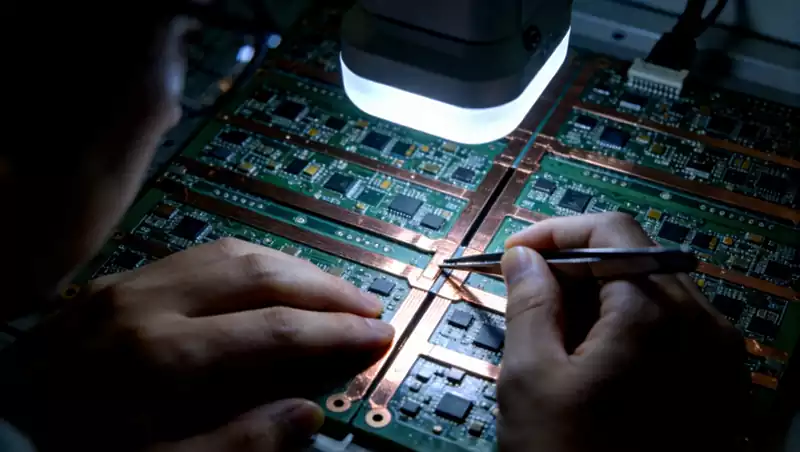
Specialised High-Precision Graphic Manufacturing
High-precision graphic manufacturing for microwave pcb boards is moving towards greater specialisation. This includes production and process control technologies for high-precision template manufacturing, high-precision graphic transfer, and high-precision graphic etching. Laser Direct Imaging (LDI) technology offers technical advantages in microwave pcb processes, addressing challenges related to alignment and graphic precision in traditional manufacturing. Additionally, reasonable manufacturing processes must be developed to meet different design requirements (such as whether holes are metallised or the type of surface coating), and extensive process experiments are needed to optimise process parameters for each related process and determine process margins.
Diversification of surface coatings
Surface coating technologies for microwave pcb is continuously evolving to accommodate expanded application ranges and complex, variable environmental conditions. Particularly due to the widespread use of aluminium substrate materials, higher requirements are placed on surface coating and protection. In addition to traditional chemical silver plating and tin-cerium alloy plating, processes such as electroplating nickel-gold are required to meet the soldering requirements of microwave devices, ensuring that microstrip patterns remain undamaged in harsh environments. Simultaneously, addressing three-proof protection technology—ensuring effective protection without compromising microwave performance—is an important research direction. Furthermore, attention must be paid to the protection and plating technologies for aluminium substrates, as unprotected aluminium substrates are prone to corrosion in humid or salt fog environments. Research into electroplating technologies for aluminium substrates is increasingly important to meet the demand for plating silver, tin, and other metals on aluminium substrate surfaces for microwave device soldering or other special applications.
CNC Machining of Microwave Printed Circuit Boards
The machining of microwave pcb boards, especially three-dimensional machining of boards with aluminium backing plates, is a key technical challenge in mass production. Conventional machining methods cannot guarantee manufacturing accuracy, consistency, and production cycle times for large quantities of microwave printed circuit boards with aluminium backing plates. Therefore, advanced computer-controlled CNC machining technology must be adopted. The mechanical processing requirements for microwave pcb is significantly higher than those for ordinary printed circuit boards, and the precision of shape processing is typically higher as well. As the shapes of microwave pcb boards become increasingly complex, with stringent dimensional accuracy requirements and large production volumes for the same product type, the application of CNC milling processing technology is necessary. When designing microwave boards, the characteristics of CNC processing must be fully considered, with all internal corners at processing points designed as rounded corners to facilitate one-step forming. The outer shape machining process is the longest process in the manufacturing of microwave printed circuit boards, and its technical level directly affects the overall processing cycle and development/production cycle of the product.
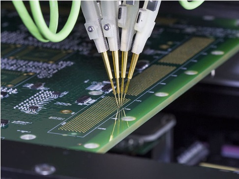
Batch production inspection equipment standardisation
Microwave pcb not only serves as structural and connecting components but more importantly as signal transmission lines. When conducting electrical testing on microwave printed circuit boards that transmit high-frequency signals and high-speed digital signals, it is not only necessary to measure whether the circuit’s ‘open,’ ‘closed,’ and ‘short circuit’ conditions meet requirements but also to verify whether the characteristic impedance values fall within specified ranges. Additionally, high-precision microwave pcb boards require extensive data verification, including graphic accuracy, positional accuracy, registration accuracy, plating layer thickness, and three-dimensional dimensional accuracy of the outer shape. Traditional inspection methods primarily rely on manual visual inspection and simple measurement tools, which struggle to meet the requirements of mass production for microwave printed circuit boards, resulting in prolonged inspection cycles and frequent errors or omissions. Therefore, the manufacturing of microwave printed circuit boards is increasingly moving toward the use of automated inspection equipment for mass production. Jingwang Electronics’ Central Laboratory has introduced over 70 advanced testing devices, capable of conducting over 40 types of inspections, placing it at the forefront of the industry. Before large-scale production, conducting a trial batch of PCB prototype boards is an important step for testing and confirming the design.
Basic requirements for high-frequency microwave pcb:
- Base material: During design, the electrical engineers have already selected the specified dielectric constant, dielectric thickness, and copper foil thickness based on actual impedance requirements. Therefore, when accepting orders, it is essential to carefully verify that these requirements are met.
- Transmission line manufacturing precision requirements: High-frequency signal transmission imposes strict requirements on the characteristic impedance of printed conductors. The manufacturing precision of transmission lines is generally ±0.02mm (±0.01mm precision transmission lines are also common). The edges of transmission lines must be extremely neat, with no burrs or notches allowed.
- Plating Requirements The characteristic impedance of high-frequency microwave pcb transmission lines directly affects the quality of microwave signal transmission. The magnitude of characteristic impedance is related to copper foil thickness, especially for microwave boards with plated-through holes. Plating thickness not only affects the total copper foil thickness but also impacts the precision of conductors after etching. Therefore, the thickness and uniformity of the plating must be strictly controlled.
- Mechanical processing requirements: First, the materials used for high-frequency microwave pcb differ significantly from those of printed circuit boards (PCBs) in terms of mechanical processing. Second, the processing precision requirements for high-frequency microwave boards are much higher than those for PCBs, with typical dimensional tolerances of ±0.1 mm (high-precision boards typically have tolerances of ±0.05 mm or 0 to -0.1 mm).
- Requirements for characteristic impedance As mentioned earlier, characteristic impedance is the most fundamental requirement for high-frequency microwavepcb. If this requirement is not met, all other efforts are in vain.