Flip Chip Bonding is a highly efficient semiconductor packaging method widely used in high performance electronic devices. This technique achieves compact package design and excellent electrical performance by inverting the chip and soldering it to the substrate.Flip chip soldering usually uses solder balls or solder joints to fix the chip to the printed circuit board (PCB) by means of the corresponding solder material.The solder material is usually an alloy solder, such as tin-lead alloy or lead-free solder, with good electrical conductivity and solderability.Flip chip is a pinless structure that generally contains a circuit unit.It is designed to be electrically and mechanically connected to a circuit by an appropriate number of solder balls (covered by a conductive adhesive) located on its face. Wire Bonding,as a connection method in Flip Chip technology, is responsible for connecting the electrical connection points of the chip to the circuitry on the PCB, making it an important part of the electronic packaging field.
Flip Chip Principle
Flip chip, also known as flip chip technology, operates on the principle of depositing tin-lead balls on the input/output (I/O) pads of integrated circuits, and then flipping the chip over and heating it up to make use of the molten tin-lead balls to bond it tightly with the ceramic substrate. This technology is gradually replacing the traditional wire bonding method, becoming the mainstream trend of future packaging technology, and is currently mainly used in high-performance CPUs, GPUs (graphics processors) and chipsets and other high-temperature products. Compared with the chip-on-board (COB), the distinctive feature of flip-chip is that its chip structure and input and output terminals (i.e., tin balls) face downwards. With inputs and outputs spread across the entire chip surface, flip-chips have reached the ultimate in package density and data processing speed. Especially important is that this technology can draw on the processing means of surface mount technology (SMT), and is therefore considered to be the ultimate development direction in the field of chip packaging technology and high-density mounting.
The manufacturing process for flip chip covers a variety of steps, including wafer heat treatment,surface metal deposition, etching, backside adhesive application, and contact lamination. Specifically, the heat treatment step is designed to optimise the crystal structure and surface flatness of the wafer; surface metal deposition is used to build electrodes on the wafer to achieve circuit connections; etching is responsible for removing excess metal to accurately form the circuit pattern; backside gluing is used to firmly adhere the chip to the substrate; and contact lamination is used to use pressure to tightly connect the chip to the circuit contacts on the substrate. The contact press is to use pressure to connect the chip and the circuit contacts on the substrate together.
Flip chip components are mainly used in semiconductor devices, but certain components such as passive filters, detector antennas, and memory devices have also begun to adopt flip chip technology. This technology has been adopted because the chips can be attached directly to the substrate and carrier by means of bumps. Therefore, Flip Chip is more precisely called DCA (Direct Chip Attach). In the diagram below, electronic products such as CPUs and memory sticks are the most common examples of devices that use Flip Chip technology.
Wire bonding is the scientific name of the lead bonding is in the semiconductor device manufacturing process, in the integrated circuit (IC) or other semiconductor devices and their packages for interconnection between the production process, the principle of the process, the use of heat, pressure, ultrasonic energy for the use of the metal leads and substrate pads tightly welded together, to achieve electrical interconnections between the chip and the substrate and the chip between the intercommunication of information. Under ideal control conditions, the lead and the substrate will occur between the electronic sharing or atomic interdiffusion, so that the two metals to achieve atomic level bonding. Wire bonding is the introduction and removal of electrical connections from the core components and plays an important role in most semiconductor device manufacturing processes.
The main principle of wire bonding is to create a thin wire between the metal pad of the integrated circuit chip and the circuit connections on the package substrate. These wires are usually made of conductive materials such as gold, aluminium or copper. The process of wire bonding consists of attaching fine wires (typically 25 to 50 microns in diameter) to the pads by ultrasonic, thermocompression or laser welding to form a stable electrical and mechanical connection. Wire bonding requires not only a strong connection, but also good electrical conductivity and corrosion resistance.
Difference between Flip Chip and Leaded Lamination
From the perspective of packaging form, flip chip adopts the packaging method that the solder joints are oriented towards the top of the PCB board, while the wire bonding package is to encapsulate the chip on the metal sheet.The position of the solder joints of the flip chip is closer to the PCB board,the chip’s heat dissipation is good, vibration and shock resistance is stronger.The leaded package is simple and low cost.
From the production process point of view, the production process of flip chip is relatively cumbersome, including wafer manufacturing process,probe measurement, cut crystal, glue dispensing, baking, welding, cleaning, testing and other aspects of the relatively high cost. The production process of the leaded Kenwood package is relatively simple, with fewer processes and relatively low cost.
From the point of view of reliability,the electrical capability of the flip chip is better than that of the leaded Kinetic package,with its extremely low resistance and inductance, able to work at a higher frequency,and higher reliability. The reliability of the leaded Kinetic package is relatively low,and it is easy to lead to mismatch and different expansion coefficients and other factors that lead to package failure.
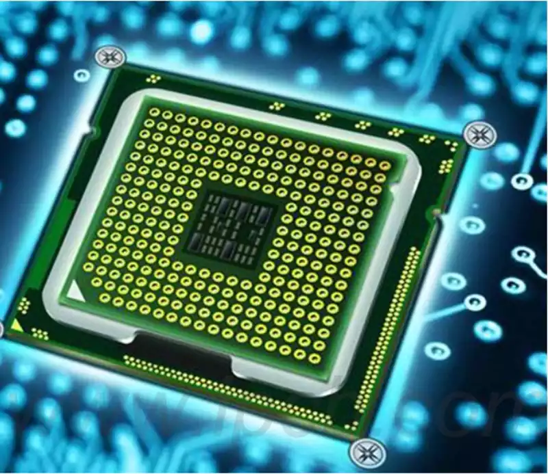
Flip chip soldering technology,the two main core of the chip bumps and flip chip soldering process, these two points are critical to the promotion of flip chip soldering technology.
(1) Bump Manufacturing
Bump manufacturing processes are diverse, including but not limited to evaporation/sputtering technology,reflow curing after solder paste printing,chemical plating, electroplating, nail head method, and ball-bumping method (SB2-Jet), etc. Each of these processes has its own advantages,but it is important to ensure that the bumps will not fail. Each of these processes is unique,but ensuring consistent bumping is key.Especially in the context of the increasing number of chip pins and increasingly stringent dimensional requirements,the size of the bumps and their spacing are constantly shrinking,while avoiding damage to the fragile chips during the production process.The current mainstream method of manufacturing bumps is to use a print/transcribe-mount-reflow-cure process. The method through the stencil printing or needle transcription technology,the chip surface uniformly coated with flux,and then through the piggyback device to accurately place the tin ball in the flux-covered solder joints, and finally into the reflow furnace for curing treatment.
(2) Flip-flop soldering
Flip-fit welding technology mainly includes fusion welding,heat pressure welding,ultrasonic welding and adhesive connection. Among them, the application of thermocompression welding and ultrasonic welding is more widely used.Thermocompression welding process requires precise placement of the chip on the substrate, while applying the appropriate pressure and temperature. The advantages of this process include ease of operation, low temperature requirements, no flux, and the ability to achieve fine-pitch connections; however, the disadvantages are that the thermal pressure is high, usually only for rigid substrates (such as alumina or silicon), and requires a high degree of flatness of the substrate, and the head of the thermal compression needs to have a high degree of parallelism. In order to avoid unnecessary damage to the semiconductor material, the equipment needs to have precise gradient pressure control. Ultrasonic hot-press welding introduces ultrasonic waves into the hot-press connection process to accelerate the welding speed. The ultrasonic waves soften the joining material quickly, making plastic deformation easier. The advantages of ultrasonic hot-press welding are that it reduces the joining temperature and shortens the processing time; however, the disadvantage is that it may leave tiny craters on the silicon wafer, which is mainly due to excessive ultrasonic vibration. Therefore, this method is mainly suitable for the combined connection of gold bumps and gold-plated pads.
The ultrasonic thermocompression soldering technique combines the advantages of ultrasonic and thermocompression connections to speed up the soldering process. The application of ultrasound induces a rapid softening of the joining material, which facilitates plastic deformation. The main advantage of thermo-ultrasonic welding is the ability to reduce the required joining temperature and significantly shorten the processing time. However, a potential disadvantage is the possibility of creating tiny craters on the surface of the wafer, which is usually caused by the excessive intensity of the ultrasonic vibrations. Therefore, the technique is particularly suitable for the paired connection of gold bumps to gold-plated pads.
Flip chip soldering and wire bonding technologies each have their own specialities in the field of semiconductor packaging.Flip chip has become the preferred choice for high-end products due to its high performance and compact packaging,while lead bonding is still popular in certain applications due to its low cost and simple process. In the future, both technologies will continue to evolve as technology continues to advance,and together they will drive innovation in the semiconductor industry.
