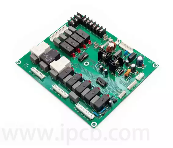
Custom PCBA refers to the customised design and production of PCBA products according to customer requirements. This includes selecting the right components for the specific application, designing a board layout that meets the requirements, and adopting appropriate processing techniques. The advantage of custom PCBA is that it can meet the specific needs of customers and provide more efficient and reliable product solutions.
Custom PCBA process:
1.Pre-preparation stage
Demand analysis and planning
Define the functional requirements: determine the specific functions that need to be achieved by PCBA, such as signal acquisition, data processing, communication and transmission.
Set performance indicators: quantify the key parameters, such as operating voltage range, current size, frequency response, accuracy requirements, etc..
Set budget and cycle time: Plan a reasonable cost budget and delivery schedule based on project requirements and market conditions.
Schematic and PCB Design
Schematic design: Use EDA software to draw circuit schematic, clarify the connection relationship of components, and ensure the correct logic of the circuit.
PCB layout and wiring: PCB layout design according to the schematic diagram, optimise the location and alignment of components, taking into account signal integrity, power distribution, heat dissipation and EMI/EMC requirements.
Design Verification: Verify the feasibility of the design through simulation and testing, and output Gerber files, drilling files and other production documents.
2.Production Preparation Stage
Component procurement and inspection
Formulate BOM list: Generate a list of components according to the design documents, specifying the model, specification and package form.
Procurement management: Select reliable suppliers to ensure the supply of genuine components and meet the performance and delivery cycle requirements.
Incoming material inspection: carry out appearance inspection and performance test on key components to prevent defective products from flowing into the production process.
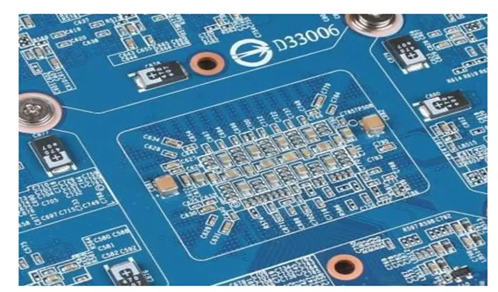
PCB Manufacturing
Submission of design documents: Transmit Gerber documents and other production information to PCB manufacturers.
Process control: Supervise the PCB manufacturing process to ensure that the board thickness, aperture diameter and other parameters meet the design requirements to avoid production defects.
3.Assembly Processing Stage
SMT SMD processing
Solder Paste Printing: Accurately apply solder paste to PCB pads through stencils.
Component Mounting: Use the mounter to mount the surface mounted components (SMC/SMD) to the specified position.
Reflow Soldering: Melt the solder paste at high temperature to achieve a solid connection between the components and the PCB.
DIP Insertion Processing
Plug-in operation: Insert plug-in components into PCB through-holes manually or by machine.
Wave soldering: Finish soldering and fixing of plug-in components by wave soldering equipment.
Post-soldering processing
Cleaning: Remove soldering residual flux and contaminants.
Curing: Enhance the mechanical strength and electrical properties of the welding point.
4.Quality Inspection Stage
Appearance and structure inspection
Appearance Inspection: Use visual tools to check PCB size, scratches, stains, bridges and other defects.
Structural inspection: Confirm the component installation position, hole accuracy and structural integrity.
Electrical performance test
AOI Inspection: Automatic optical inspection of soldering quality and component location.
ICT test: Verify electrical parameters such as circuit on/off, voltage and current.
FCT test: Simulate the actual environment to test the overall function of PCBA.
Reliability Test
Aging test: long-time power operation to observe the failure.
Fatigue test: high frequency operation to verify the functional stability.
Environmental testing: Exposure to extreme temperature and humidity, vibration and other conditions to test the reliability.
- Post-processing stage
Protection and Packaging
Coated with three-proof paint: to achieve moisture-proof, dust-proof and corrosion-proof protection.
Anti-static packaging: using special materials to avoid static damage.
Delivery and after-sales
Delivery of finished products: Hand over qualified products to customers or enter the next assembly process.
After-sales support: Provide maintenance services, handle user feedback and continuously optimise designs.
Custom PCBA is becoming the development trend in the field of electronic manufacturing with its advantages of precise matching of demand, excellent quality assurance, one-stop service experience and leading industrial innovation. For enterprises, choosing a professional custom PCBA supplier will help them stand out in the fierce market competition and achieve product differentiation competition and innovative development. In the future, with the continuous progress of technology and changing market demand, custom PCBA will certainly usher in a broader development prospect, and make greater contribution to promoting the upgrading and development of the electronics industry.