Why FMC Connector PCB Layout Often Determines System Limits
In high-speed digital system design, many performance issues don’t originate with the chip itself, but rather occur in the very first step after the chip leaves its package. The FMC connector is precisely such an easily underestimated yet highly critical interface component. When a system operates in a high-speed, high-bandwidth, high-concurrency signal environment, the PCB layout related to the FMC connector often directly determines the stability of the entire platform.
Functionally, the FMC connector wasn’t designed for simple signal connection, but rather to provide a standardized interface for modular, high-speed expansion. It’s commonly found in FPGA development boards, accelerator cards, and various reconfigurable computing platforms, used to connect daughter cards, functional modules, or external high-speed devices. This application context naturally dictates that the FMC interface carries complex, dense, and high-speed signals.
Therefore, the PCB layout of the FMC connector cannot be treated like a “normal connector” from the outset. It deals not with single-function signals, but with a complex structure that mixes high-speed differential signals, clock signals, power supplies, and ground references. If the layout phase is not handled properly, even using high-performance chips later will hardly compensate for inherent signal quality defects.
In real-world projects, many engineering problems often don’t stem from connectivity issues, but rather from system stability and edge performance. For example, a system might function normally in a laboratory environment, but begin to exhibit intermittent errors after temperature changes, load variations, or speed increases. The root cause of these problems often lies hidden in the PCB layout details near the FMC Connector, including trace structure, reference plane continuity, and subtle changes in impedance.
More importantly, the FMC interface is typically located at the system’s “boundary.” It must maintain a high degree of compatibility with the motherboard’s core logic while also being compatible with the uncertainties of external modules. This dual constraint makes FMC Connector PCB layout not just a single-board design issue, but part of system-level signal integrity design.
From an engineering experience perspective, once a problem is introduced in the FMC interface layout phase, there are almost no low-cost solutions for later correction. In contrast, systematic planning of the FMC Connector area from the early design stages can significantly reduce debugging risks and shorten the overall development cycle.
Therefore, discussing FMC connector PCB layout isn’t about how a single trace should be routed, but rather about whether engineers truly understand the interface’s role in a high-speed system architecture and whether the PCB is treated as “part of the circuitry.”
How FMC Connector Signal Characteristics Constrain PCB Layout
To truly understand why FMC connector PCB layout is so sensitive, we must first return to the original design intent of the FMC interface itself. FMC wasn’t designed for low-speed or single-function signals, but rather for achieving multi-channel, high-speed, scalable modular interconnects within a limited space. This design goal fundamentally determines its stringent requirements for PCB layout.
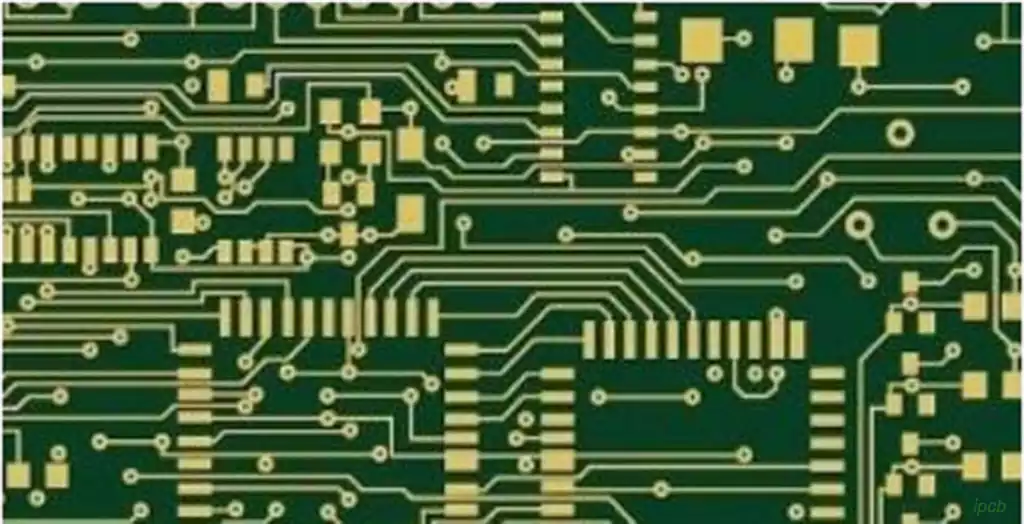
FMC interfaces typically need to carry a large number of high-speed differential signals, often directly from the I/O resources of FPGAs or high-speed processors. In such scenarios, the signal rate is already high enough; high-frequency effects are no longer a peripheral issue but a core factor determining system usability. Signals passing through the FMC connector not only experience impedance changes from the device itself but are also affected by PCB traces, vias, and changes in the reference plane.
From a signal integrity perspective, the PCB layout of the FMC interface area is not a simple extension, but a highly sensitive transition zone. While the routing environment on the chip side is relatively controllable, the connector itself introduces structural discontinuities. If the PCB layout cannot provide a stable and continuous impedance environment for these high-speed signals, reflections, crosstalk, and even mode switching problems will occur in this transition zone. These problems often do not immediately lead to system failure, but they significantly compress the system’s performance margin.
Power and ground distribution is also a constraint that cannot be ignored in FMC connector PCB layout. The FMC interface typically provides power support for external modules, and these power supplies often need to be distributed and decoupled near the interface. If the power return path is not designed properly, it will not only affect the power supply stability of the module, but may also indirectly interfere with high-speed signals through ground bounce noise. This “invisible coupling” is particularly common in high-speed systems.
Furthermore, the signal types of the FMC interface are highly mixed, which is also a significant reason for the increased layout complexity. High-speed differential signals, single-ended control signals, clock signals, and power signals are often highly concentrated in the same interface area. If the PCB layout fails to partition the space reasonably, mutual interference between different signals will be inevitable. At this point, even if the design of a single signal is “correct,” the overall system may still exhibit instability.
From an engineering practice perspective, the signal characteristics of FMC Connectors do not simply require “shorter, straighter” traces. Instead, designers must clearly define during the layout phase which signals are most sensitive to impedance continuity, which areas cannot arbitrarily interrupt the reference plane, and which vias and layer transitions must be handled with caution. This proactive understanding is often more valuable than later simulation and debugging.
Therefore, the constraints on FMC Connector PCB layout are not artificially added complexity, but rather engineering realities determined by the signal characteristics of the interface itself. Ignoring these constraints is tantamount to gambling system stability on luck.
The Core Logic of High-Speed Differential Signal Layout in the FMC Connector Area
In FMC Connector-related PCB designs, high-speed differential signals almost always represent the highest performance risk and require the highest priority. The problem is not whether engineers know that differential pairs must be of equal length and impedance controlled, but rather that these principles are often simultaneously constrained by multiple structural limitations in the FMC interface area, making the “correct approach” less intuitive.
First, it’s important to clarify that high-speed differential signals are not isolated near the FMC Connector. They are constrained by both the chip-side I/O layout and the connector’s pin arrangement. This dual constraint means that differential pairs are already in a highly compressed routing environment before even entering the connector area. If sufficient routing paths are not reserved at this stage, subsequent length and spacing controls often come at the cost of sacrificing the integrity of the reference plane.
The continuity of the reference plane is one of the most easily overlooked yet most impactful factors in FMC Connector PCB layout. The dependence of high-speed differential signals on the reference plane is not only reflected in impedance calculations but also in whether the return path is forced to detour. Once a differential signal crosses a split ground or power plane in the connector area, its return path will change uncontrollably, leading to reflections and common-mode noise. These issues are not always explicit in simulations but often emerge in actual testing.
The use of vias is also a critical point in layout. To achieve inter-layer switching, differential signals inevitably need to enter the FMC Connector through vias. However, each via introduces additional parasitic parameters, especially in high-speed scenarios where the via itself becomes part of the signal path. If there are too many vias or the structure is asymmetrical, even if the differential pairs maintain good matching on the planar traces, significant signal distortion may occur in the interface area.
Furthermore, the “controllability” of differential signals in the FMC interface area is often lower than in other areas of the board. The size and arrangement of the connector pads, as well as the surrounding solder mask structure, can all affect the impedance environment. This means that engineers need to accept the reality during the layout phase: ideal impedance cannot be achieved at all locations, and the design goal should be to minimize the number of discontinuities and concentrate them in predictable locations.
From a system perspective, the layout of high-speed differential signals in the FMC Connector area is essentially a form of “risk management.” It’s not about pursuing absolute perfection, but about ensuring the most stable and controllable critical path within limited space and given interface conditions. A successful FMC Connector PCB layout is often not the neatest one, but the one with the most predictable signal behavior.
Therefore, the layout logic of high-speed differential signals should not be understood as a set of fixed rules, but rather as a comprehensive trade-off between interface structure, signal characteristics, and system objectives. This ability to make trade-offs is a key differentiator between experience-based design and mature engineering design.
Typical Misconceptions and Hidden Risks in FMC Connector PCB Layout
In actual engineering, problems related to FMC connectors are often not due to a complete lack of understanding of high-speed design principles, but rather to choices made under complex constraints that appear reasonable but are actually problematic. These choices may not be obvious at individual points, but they accumulate gradually at the system level, ultimately manifesting as debugging difficulties, insufficient stability, or inability to deliver performance.
A common misconception is treating the FMC connector area as a regular connector. In the initial layout phase, designers often focus on critical traces near the main chip, opting for a “connectivity as much as possible” strategy in the interface area. This ignores the fact that for high-speed systems, the area near the connector is where signal structure changes most drastically. Relaxing requirements here is equivalent to reducing protection at the system’s most vulnerable point.
Another easily underestimated problem is the passive destruction of the reference plane. To make way for connector pads, mounting holes, or mechanical structures, the ground or power planes are often fragmented. While this fragmentation has limited impact in low-speed systems, in high-speed, high-density areas like FMC interfaces, it directly forces signal return paths to detour, introducing additional noise and uncertainty. More problematic is that these issues often don’t reproduce consistently in a single test, making troubleshooting exceptionally difficult.
Via design is also a significant source of hidden risks. To meet the fan-out requirements of dense pins, differential signals frequently switch layers, rapidly increasing the number of vias. If the via structure isn’t uniformly planned, or if differential pairs are asymmetrical at via locations, unpredictable signal distortion can be introduced into the connector area. This distortion isn’t always apparent during simulation but is amplified during high-speed operation or changes in boundary conditions.
Furthermore, improper signal mixing is a common problem in FMC connector PCB layouts. Excessive spatial interweaving of high-speed differential signals with low-speed control signals and power traces may seem to save routing space, but it actually increases crosstalk and coupling risks. In the interface area, the impact of this mixed layout is further amplified because the signal is already in a structurally discontinuous environment, significantly reducing its anti-interference capability.
The last often overlooked misconception is the underestimation of “tunability.” Once an FMC interface problem is exposed, it is often difficult to resolve with simple modifications. If necessary testing and observation methods are not reserved during the layout phase, later debugging can only rely on indirect inference, greatly extending the development cycle. This is not due to a lack of technical ability, but rather a result of insufficient system risk assessment during the layout phase.
These misconceptions recur not because engineers are unprofessional, but because the FMC Connector PCB layout itself is at the intersection of multiple constraints. Only by prioritizing system stability during the design phase and proactively identifying and mitigating these hidden risks can the true value of the FMC interface in high-speed systems be realized.
Summary | The Key Value of FMC Connector PCB Layout
Reviewing the preceding sections, from the signal characteristics of FMC Connectors to layout constraints, high-speed differential signals, and common misconceptions, we can clearly conclude one core point: FMC Connector PCB layout is not simply a routing issue, but the foundation of the reliability and performance of the entire high-speed system. PCB layout not only provides physical connections but also forms the first line of defense for signal integrity, power integrity, and system stability. The length matching of high-speed differential signals, reference plane continuity, via optimization, and mixed-signal management—every design choice can impact the overall system performance.
In real-world projects, any compromises made during the layout phase can amplify problems during debugging, leading to extended development cycles and substandard performance. Therefore, design decisions for the FMC connector area should be based on a comprehensive understanding of signal behavior, system requirements, and potential risks.
Ultimately, the value of FMC Connector PCB layout lies not only in the availability of connectivity but also in its profound guarantee of system performance. Understanding and mastering these layout principles is an essential core competency for high-speed electronic systems engineers and a crucial basis for purchasing and product decision-makers to identify reliable solutions.