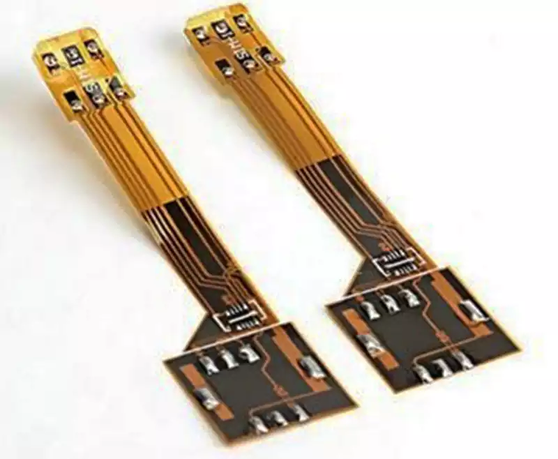
The PCBA assembly and soldering process for FPCs differs significantly from that of rigid circuit boards. Due to their insufficient rigidity and flexibility, FPCs cannot be secured or transported without specialized carrier boards, rendering essential SMT processes like printing, component placement, and reflow soldering impossible.
PC Pre-Treatment
FPC boards are flexible and typically not vacuum-sealed upon shipment. They readily absorb moisture from the air during transportation and storage. Therefore, pre-baking is required before SMT production to slowly and forcibly expel moisture. Otherwise, under the high-temperature shock of reflow soldering, absorbed moisture rapidly vaporizes into steam that escapes from the flexible pcb, potentially causing delamination, bubbling, and other defects.
Typical pre-bake conditions are 80-100°C for 4-8 hours. In special cases, temperature may be increased to 125°C or higher, but baking time must be correspondingly reduced. Always conduct small-scale trials before baking to verify flexible pcb board tolerance for the set temperature. Avoid stacking excessive flexible board layers during baking; with 10-20 PNLs being optimal. Some flexible pcb manufacturers insert paper sheets between each PNL for separation. Verify that these separation sheets can withstand the set baking temperature. If not, remove the separation sheets before baking. Post-baked flexible boards should show no significant defects such as discoloration, deformation, or warping. Only after passing IPQC random inspection can they be released for production.
Custom Carrier Plate Fabrication
Based on the PCB CAD files, extract the flexible circuit board hole positioning data to manufacture high-precision flexible pcb boards positioning templates and custom carrier plates. Ensure the diameter of the positioning pins on the template matches the hole diameters on both the carrier plate and the flexible pcb. Many FPCs feature non-uniform thickness due to circuit protection or design requirements—some areas are thicker, others thinner, and some incorporate reinforced metal plates. Consequently, the interface between the carrier board and flexible pcb requires machining, grinding, and slot cutting tailored to actual conditions. This ensures the flexible circuit boards remains flat during printing and component placement. Carrier board materials must be lightweight, thin, high-strength, low-heat-absorption, and fast-cooling, with minimal warping or deformation after repeated thermal shocks. Common carrier materials include synthetic stone, aluminum plates, silicone rubber sheets, and specialized high-temperature magnetic steel plates.
Synthetic Stone Carrier Plates (Commonly Used)
Advantages: Easy design, rapid prototyping, lifespan of approximately 4,000–7,000 cycles, user-friendly operation, good stability, low heat absorption, cool to the touch, cost-effective.
Disadvantages: Asynchronous heat absorption between carrier and flexible pcb boards (though the difference is not significant). Commonly used.
Aluminum Substrate Carriers (Not Recommended)
Rapid heat absorption, minimal internal/external temperature differential, synchronized heat absorption with flexible pcb boards, easily repairable deformation, low cost, long lifespan.
Disadvantages: Hot to the touch, requires insulated gloves or double-layer protective gloves for handling, prone to deformation.
QFN packaging currently encompasses an extensive range of chip manufacturing processes, with successful mass production experience even for chips manufactured using 28nm technology. Leveraging these advantages, the market holds strong confidence in QFN’s broader adoption across mid-range and high-end chips.
Alloy Material Fixtures (Recommended)
Alloy fixtures: A newer reflow fixture type gaining industry-wide recognition. Features rapid heat absorption, minimal internal/external temperature differential, synchronized heating with flexible board, low deformation risk, cost-effectiveness (comparable to synthetic stone), and extended lifespan exceeding 15,000 cycles (excluding exceptional cases). Disadvantages: Hot to the touch, requiring heat-resistant gloves or double-layer protective gloves for handling.
Silicone Sheet Carriers (Not Recommended)
Features self-adhesive properties, allowing FPCs to adhere directly without tape. Easy removal with no residue, and high-temperature resistance. Disadvantages: Adhesive strength diminishes over time, short lifespan (approximately 1,000–2,000 cycles), and higher cost.
Production Process
FPC Fixation
Before commencing SMT (Surface Mount Technology) operations, the primary step is to precisely secure the flexible printed circuit board onto the carrier board. Particular attention must be paid to minimizing the storage time between flexible circuit board fixation on the carrier board and subsequent processes such as printing, component placement, and soldering.
Carrier boards are categorized into two types: those with locating pins and those without. For carrier boards without positioning pins, a positioning template with pins must be used. The procedure involves: first, placing the carrier board over the positioning pins on the template, ensuring the pins pass through the carrier board’s positioning holes and protrude outward. Next, individually place each FPC over the exposed positioning pins and secure them with tape. Finally, separate the carrier board from the FPC positioning template to proceed with printing, placement, and soldering operations.
For carrier boards with positioning pins, several spring-loaded pins approximately 1.5mm long are pre-installed. During operation, FPCs can be directly placed onto these pins one by one and secured with tape. During the printing process, the spring-loaded pins can be fully pressed into the carrier board by the stencil, causing no impact on printing quality.
Solder Paste Printing for FPC
FPCs impose no particularly stringent requirements on solder paste composition. Parameters like tin ball particle size and metal content are primarily determined by whether the FPC incorporates fine-pitch ICs. However, FPCs demand high standards for solder paste printability. The solder paste must exhibit excellent thixotropy, enabling effortless printing release while securely adhering to the FPC surface. This prevents issues like stencil clogging due to poor release or solder paste collapse after printing.
Since the FPC is mounted on a carrier board with high-temperature-resistant positioning tape applied, its surface is not uniformly flat. Consequently, the printing surface of the FPC lacks the consistent flatness, thickness, and hardness found on PCBs. Therefore, metal squeegees are unsuitable for printing; instead, polyurethane squeegees with a hardness of 80-90 degrees should be selected. Additionally, the solder paste printer should ideally be equipped with an optical positioning system; otherwise, printing quality will be significantly compromised. Although the FPC is fixed to the carrier board, a slight gap always exists between them—the most significant difference from rigid PCBs. Consequently, equipment parameter settings also significantly impact printing results.
The printing station is critical for preventing FPC contamination. Operators must wear finger cots, maintain station cleanliness, and regularly wipe the stencil to prevent solder paste from contaminating the FPC’s gold fingers and gold-plated buttons.
FPC Component Placement
Based on product characteristics, component count, and placement efficiency, both medium- and high-speed placement machines are suitable. Since each FPC features optical MARK positioning marks, SMD placement on FPCs differs little from placement on PCBs. Note that although FPCs are mounted on carrier boards, their surfaces cannot match the flatness of rigid PCBs. Local gaps inevitably exist between FPCs and carrier boards, necessitating precise settings for nozzle descent height and air pressure, along with reduced nozzle movement speed. Additionally, since FPCs are predominantly assembled on carrier boards and exhibit relatively low yield rates, it is common for a partial PNL to contain defective PCS. This necessitates that the placement machine be equipped with BAD MARK recognition functionality. Otherwise, when producing such non-complete PNLs where all boards are good, production efficiency will be significantly compromised.
Reflow Soldering for FPCs
A forced convection hot-air reflow oven should be used to ensure more uniform temperature distribution across the FPC, thereby reducing soldering defects. When using single-sided adhesive tape, which only secures the FPC’s four edges, the central portion may deform under hot air conditions. This deformation can cause pads to tilt, allowing molten solder (liquid tin at high temperatures) to flow and result in cold solder joints, bridging, or solder balls, leading to higher process defect rates.
1) Temperature Profile Testing Method: Due to varying heat absorption properties of carrier boards and different component types on the FPC, their heating rates and absorbed heat during reflow differ significantly. Therefore, meticulous configuration of the reflow oven’s temperature profile greatly impacts soldering quality. A reliable approach involves placing two carrier boards with FPCs before and after the test board, spaced as in actual production. Components are mounted on the FPC of the test board. Test probes are soldered to test points using high-temperature solder wire, and probe leads are secured to the carrier board with high-temperature resistant tape. Note: The tape must not cover the test points. Test points should be selected near solder joints along the carrier board edges or QFP pins, as such placements yield results more representative of actual conditions.
2) Temperature Profile Configuration During oven temperature tuning, due to FPC’s poor thermal uniformity, it is advisable to adopt a temperature profile with distinct heating/holding/reflow stages. This facilitates easier control of parameters across temperature zones while minimizing thermal shock effects on both FPC and components. Based on experience, it is best to set the oven temperature to the lower limit of the solder paste technical requirements. The reflow oven airflow speed should generally be set to the lowest speed the oven can accommodate. The reflow oven chain must be stable and free of vibration.
FPC Inspection, Testing, and Depaneling
Since carrier boards absorb heat during reflow, especially aluminum ones, they exit the oven at elevated temperatures. Installing forced-air cooling fans at the exit is recommended to accelerate cooling. Operators must wear heat-resistant gloves to prevent burns from hot carrier boards. When removing soldered FPCs from carrier boards, apply even pressure without excessive force to avoid tearing or creasing the FPC.
Inspect removed FPCs under a magnifier with at least 5x magnification, focusing on residual adhesive, discoloration, solder contamination on gold fingers, solder balls, IC pin solder voids, and bridging. Due to inherent surface irregularities, AOI inspection yields high false-positive rates and is generally unsuitable for FPCs. However, specialized test fixtures enable ICT and FCT testing.
Since most FPCs are interconnected panels, depaneling may be required before ICT or FCT testing. While blades or scissors can perform depaneling, they result in low efficiency, poor quality, and high scrap rates. For high-volume production of irregularly shaped FPCs, it is recommended to create specialized FPC punching separation dies. Punching significantly improves efficiency while producing clean, aesthetically pleasing edges. The low internal stress generated during punching effectively prevents solder joint cracking.
During the assembly and soldering of PCBA flexible electronics, precise positioning and securing of the FPC are critical. The key to effective securing lies in creating a suitable carrier board. Subsequent steps include FPC pre-baking, printing, component placement, and reflow soldering. Clearly, FPC SMT processes present significantly greater challenges than rigid PCB manufacturing. Therefore, precise parameter setting is essential, alongside rigorous production process management. Operators must strictly adhere to every SOP stipulation. Line engineers and IPQC personnel should intensify patrol inspections to promptly identify production line anomalies, analyze root causes, and implement necessary corrective actions. Only through such measures can the defect rate on FPC SMT production lines be controlled within the tens of PPM range.
During PCBA production, numerous machines are required to assemble a single board. The quality level of a factory’s equipment often directly determines its manufacturing capability.
Essential equipment for PCBA production includes solder paste printers, pick-and-place machines, reflow ovens, AOI inspection systems, component trimmers, wave soldering machines, solder pots, board washers, ICT test fixtures, FCT test fixtures, and aging test racks. The specific equipment configuration varies depending on the scale of the PCBA manufacturing facility.
FPC PCBA assembly and soldering processes are complex and demanding, requiring precise control of process parameters at every stage while relying on compatible equipment support. Only through such meticulous management can defect rates be reduced, manufacturing capabilities enhanced, and steady progress achieved in the electronics market.
