FR4 PCBs (glass fiber–reinforced epoxy laminate boards), as the most widely used type of printed circuit board, have production efficiency and cost control that directly impact overall product competitiveness. Depanelization, as a critical step in the PCB manufacturing process, achieves an optimized balance among mass-production efficiency, product quality, and manufacturing cost through systematic process design.
FR4 PCBs are typically manufactured in panelized form, with the primary objective of improving processing efficiency and controlling cost. Proper panel design significantly reduces pick-and-place operations during SMT, ensures soldering consistency, and minimizes substrate material waste, thereby enabling cost-effective large-scale production. As the final and decisive step in panelized manufacturing, depanelization aims to separate individual boards from the panel quickly and accurately without compromising the original performance of each PCB. This process must satisfy three core requirements:
Edge quality, with no chipping, debris, or burrs, and edge flatness controlled within 0.2 mm;
Circuit and component safety, ensuring that depanelization does not damage components, traces, or solder joints, and avoiding pad lifting or trace breakage;
Balanced efficiency and cost, with depanelization methods matched to production volume while reasonably controlling equipment investment and labor cost.
FR4 PCB Depanelization Methods
1.V-Cut Depanelization
V-cut depanelization is the most commonly used mechanical method. During panel fabrication, a V-groove is cut between individual boards using a V-cut machine, leaving a small residual web. During depanelization, mechanical force (manual snapping or machine breaking) is applied to fracture the remaining web and separate the boards. Key parameters include groove depth and angle. Typical designs use a groove depth of one-third to one-half of the board thickness, a groove angle of 30°–45°, and a residual web thickness of 0.6–0.8 mm for standard 1.6 mm boards. This balance maintains panel rigidity while allowing easy separation.
Advantages:
High efficiency: V-cutting is completed during panel fabrication, and separation requires only a simple breaking step, enabling thousands of boards per hour per machine.
Low cost: Equipment and tooling costs are significantly lower than other methods.
Good edge quality: Fracture surfaces are relatively flat with minimal burrs, often requiring no secondary finishing.
Limitations:
Applicable only to rectangular or regular-shaped boards with straight separation lines.
Not suitable for irregular shapes.
Mechanical stress during separation may cause slight deformation in thin FR4 boards (thickness < 1.0 mm), requiring dedicated fixtures to reduce stress.
Typical applications: Medium- to high-volume production of regular-shaped FR4 PCBs with thicknesses of 0.8–2.0 mm, such as power boards and general control boards in consumer electronics.
2.Tab Routing / Mouse-Bite Depanelization
Mouse-bite depanelization (also known as perforated tab depanelization) uses evenly spaced small holes between individual boards or between boards and the panel frame, forming a structure similar to postage stamp perforations. During depanelization, mechanical force breaks the small connecting bridges between holes. Typical parameters include hole diameters of 0.8–1.2 mm, hole spacing of 1.5–2.0 mm, and bridge widths of 0.5–1.0 mm. Hole placement must avoid components and traces and be at least 2 mm from the board edge to prevent edge cracking.
Advantages:
High design flexibility, suitable for FR4 PCB of any shape, especially irregular geometries such as circular, curved, or complex outlines.
Good panel rigidity during transport and processing, making it suitable for both thin and thick FR4 boards.
Disadvantages:
Residual mouse-bite marks remain on the edges after separation, often with minor burrs; high-precision applications may require secondary edge finishing.
Lower efficiency than V-cut depanelization; dedicated depaneling machines are recommended for volume production.
Typical applications: Irregular-shaped boards, thin (<0.8 mm) or thick (>2.0 mm) FR4 PCBs, and medium-volume production, such as automotive sensor boards and customized industrial control boards.
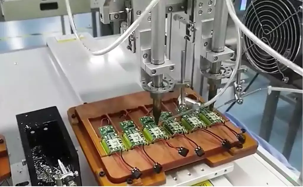
3.Router (CNC) Depanelization
Router depanelization, also known as CNC depanelization, uses a numerically controlled milling cutter to follow a predefined path along the board outline, precisely separating individual boards from the panel. The key advantage is high precision, with positioning accuracy of up to ±0.05 mm. Complex shapes can be accurately processed, and the resulting edges are smooth and burr-free, typically requiring no secondary finishing. Mechanical stress during routing is relatively low, minimizing the risk of board deformation or component damage.
Limitations:
High equipment cost, typically five to ten times that of V-cut machines.
Lower throughput, with only a few hundred boards per hour per machine.
Dust generation during routing requires effective vacuum extraction to prevent contamination of the FR4 PCB surface.
To improve efficiency, multi-spindle routing or optimized panel layouts with shorter cutting paths are often used in volume production.
Typical applications: High-precision FR4 PCBs, complex outlines, component-dense boards with components close to edges, and small- to medium-volume production, such as medical electronics, high-end communication modules, and precision sensors.
4.Laser Depanelization
Laser depanelization uses high-energy laser beams—typically UV lasers—to cut along the separation path, separating the FR4 substrate through thermal or photochemical effects. Its primary advantage is extremely high precision, with cutting accuracy up to ±0.01 mm and very narrow kerf widths (as small as 0.1 mm). This method is ideal for micro-sized FR4 PCBs (e.g., boards smaller than 10 mm × 10 mm). Being a non-contact process, laser depanelization introduces no mechanical stress, making it particularly suitable for ultra-thin FR4 boards (<0.5 mm) and rigid-flex constructions. Edges are smooth, clean, and free of burrs or dust, eliminating the need for post-processing.
Disadvantages:
Very high equipment cost, typically two to three times that of CNC depaneling machines.
Low throughput, often limited to only dozens of boards per hour, restricting its use to small-batch, high-precision applications.
Potential heat-affected zones (HAZ); improper parameter settings may cause edge carbonization and degrade insulation performance. HAZ is typically controlled below 50 μm by optimizing laser power, frequency, and cutting strategy.
Typical applications: Micro-sized and ultra-thin FR4 PCBs, high-precision electronic devices, and small-batch production, such as wearable electronics, micro-sensors, and advanced chip packaging substrates.
5.Manual Depanelization
Manual depanelization uses hand tools such as scissors, pliers, or utility knives to separate boards. Its only advantage is minimal equipment cost, making it suitable for very small quantities (typically dozens of boards or fewer) with simple shapes.
Disadvantages:
Low precision and poor edge quality, with a high risk of chipping, burrs, and damage to components or traces.
Low efficiency and poor consistency, making quality control difficult.
Manual depanelization is therefore limited to prototyping and trial production and is not suitable for mass production.
Common Depanelization Issues and Solutions
Issue 1: Edge chipping or debris after depanelization
Causes: Mismatch between depanelization method and board thickness (e.g., using V-cut on thin boards), insufficient V-groove depth, or overly narrow mouse-bite bridges.
Solutions: Change to a suitable method (e.g., mouse-bite for thin boards), optimize V-cut depth to one-third to one-half of board thickness, or increase bridge width to 0.8–1.0 mm.
Issue 2: Board warpage after depanelization
Causes: Excessive mechanical stress during separation (manual or unsupported V-cut depanelization) or asymmetric panel layouts.
Solutions: Use dedicated depaneling fixtures, select low-stress methods (router or laser depanelization), and optimize panel layouts to ensure symmetry and balanced mass distribution.
Issue 3: Component damage or solder joint failure
Causes: Mechanical force transmitted to components during separation or depaneling paths too close to components.
Solutions: Increase the distance between depaneling paths and components (≥3 mm), use non-contact methods such as laser depanelization, and add local reinforcement features to distribute stress.
Issue 4: Edge carbonization after laser depanelization
Causes: Excessive laser power or slow cutting speed, resulting in an oversized heat-affected zone.
Solutions: Optimize laser parameters by reducing power and increasing speed, use UV lasers with smaller HAZ, and apply multiple shallow passes instead of a single deep cut.
Although FR4 PCB depanelization occurs at the final stage of the manufacturing process, it directly determines final product quality and production efficiency. The value of each depanelization method lies in its suitability for specific application scenarios. The core selection principle is not to pursue the “most advanced” or the “lowest cost” approach, but to identify the optimal balance among quality, efficiency, and cost.