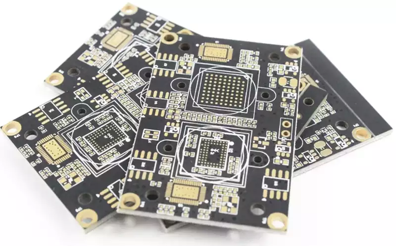
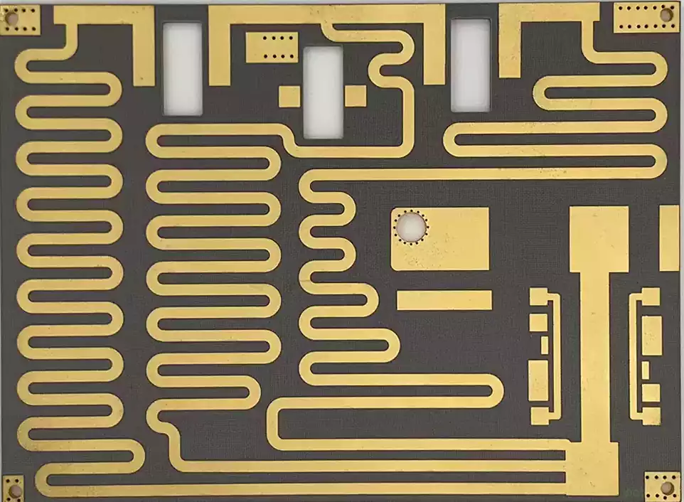
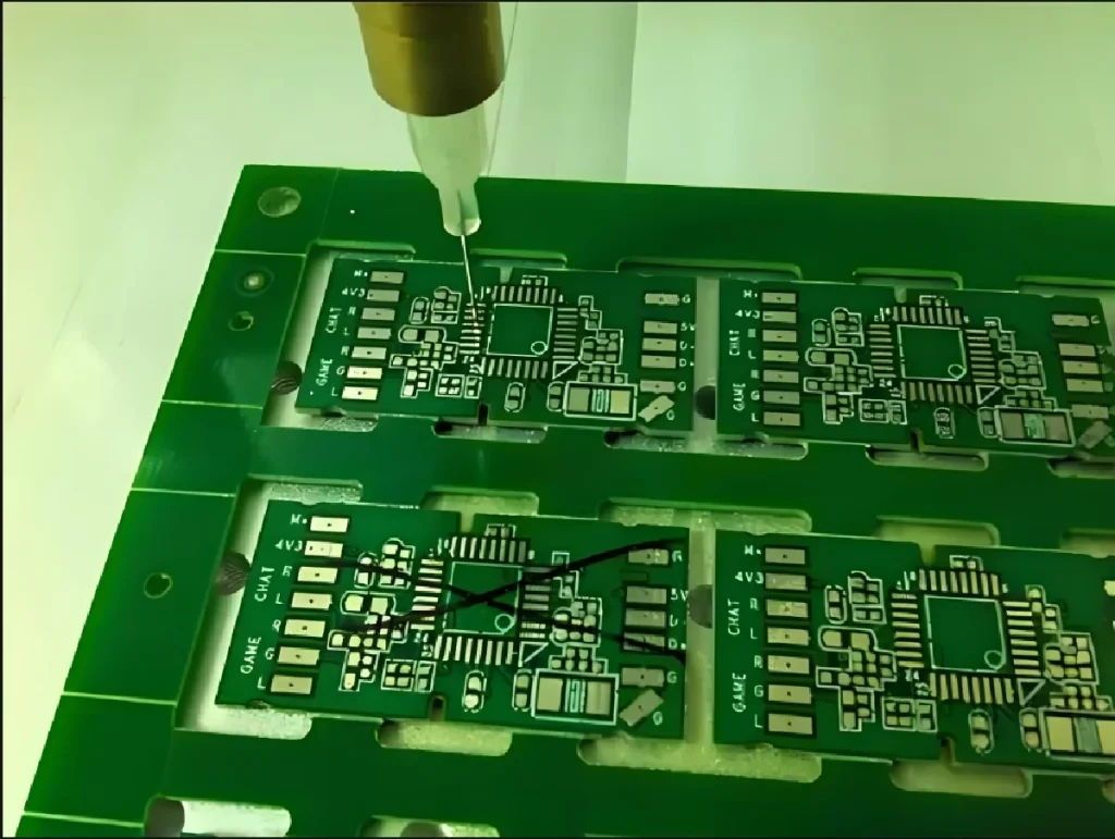
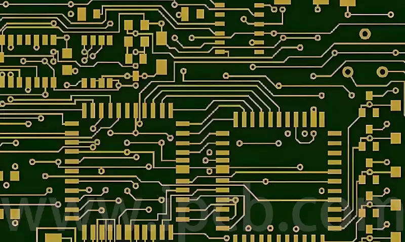
Glass pcb and their derivatives, glass through hole (TGV) carrier board,has become indispensable core components for various high-tech electronic products. They are not only widely used in liquid crystal display (LCD),organic light-emitting diodes (OLED) and other display technologies,but also play an important role in semiconductor packaging, integrated circuit interconnections and other aspects.
Mainstream manufacturing techniques for glass pcb:
The manufacturing of glass pcb mainly relies on three techniques,namely float,flow-hole pull-down and overflow melting,with overflow melting being the most popular.
Float manufacturing technology,as the longest history of flat glass manufacturing and the most widely used technology,the process is the molten glass from the kiln into the continuous flow,and make it float in the relatively high density of the tin liquid surface.Under the combined effect of gravity and surface tension, the glass spreads out on the tin surface to form a glass with flat top and bottom surfaces,which is cooled and led onto a transition roller table.The advantages of the float process are its high capacity and the ease of scaling up the size of the substrate glass.
Flow Hole Pull Down is a technique in which molten glass is channelled into a flow hole funnel made of a platinum alloy.Under the force of gravity,the glass solution flows out of the flow holes and is then crushed by rollers and cured in a cooling chamber to form the final shape.In this process,the temperature and the opening size of the flow holes together determine the yield of the glass,while the opening size of the flow holes and the pull down speed together determine the thickness of the glass,and the temperature distribution determines the flatness of the glass.
Overflow melting is a technique in which molten glass is channelled into a conduit.When the glass reaches the upper volume limit of the catheter, it overflows down the walls of the catheter from both sides,like a waterfall,and pools underneath to form a sheet-like substrate.The overflow melting technology is capable of producing ultra-thin glass substrate with double original glass surfaces, and compared to float and flow-hole downdrawing,it eliminates the need for post-processing fabrication processes such as grinding or polishing.Therefore,it has become the mainstream technique for TFT-LCD substrate glass manufacturing.
Glass through hole (TGV) carrier board Process Flow Details
Starting from the preparation of the glass pcb,this step requires very high quality of the glass substrate to ensure that it has a high degree of flatness,high cleanliness and good thermal stability,while the size and thickness need to be precisely controlled.Contaminants are thoroughly removed from the surface of the substrate by specialised cleaning equipment.
Subsequently,glass drilling is carried out,using high precision laser drilling equipment to form penetrating holes in the substrate,strictly controlling the laser parameters and drilling speed to ensure that the location,diameter and shape of the holes comply with the design requirements,and the hole shape is often designed as a conical shape,which is convenient for subsequent processing.
Then the hole wall metallisation treatment,the use of PVD or CVD process in the hole wall to form a conductive metal seed layer,the need to choose the right metal material and deposition parameters to ensure that the uniformity of the metal layer and conductivity.
Photolithography is a key step,need to be coated with photoresist on the surface of the substrate,through the photolithography machine will be transferred to the circuit pattern on the photoresist,strict control of photolithography parameters and exposure time,to ensure that the pattern accuracy and clarity. Subsequently,the developer is used to expose the parts that do not need plating.
Hole filling using plating process,the conductive material filled into the hole,the formation of conductive pathway,need to choose the appropriate plating solution and parameters to ensure that the filling is complete and no voids,and post processing to improve conductivity and stability.
After the completion of the filling,the glass pcb surface flattening treatment to remove residues and repair unevenness,achieved through chemical or mechanical polishing,need to strictly control the polishing parameters and time.
Finally, on the surface of the substrate to form a protective layer and terminal connections,the protective layer is made of polymer materials to protect the circuit from external influences,the terminal connections using professional welding equipment to weld the pins to the corresponding position of the carrier board to ensure that the circuit works properly.
The glass through hole (TGV) carrier board process is complex and delicate,requiring strict control of process parameters and quality requirements to ensure the performance and quality of the final product.
With the continuous progress of science and technology,the application of glass pcb and their derivatives glass throughhole (TGV) carrier boards in high-tech electronic products will have a broader prospect. Strict control of the manufacturing process to ensure product performance and quality will be the key to driving the continued development of this field.
