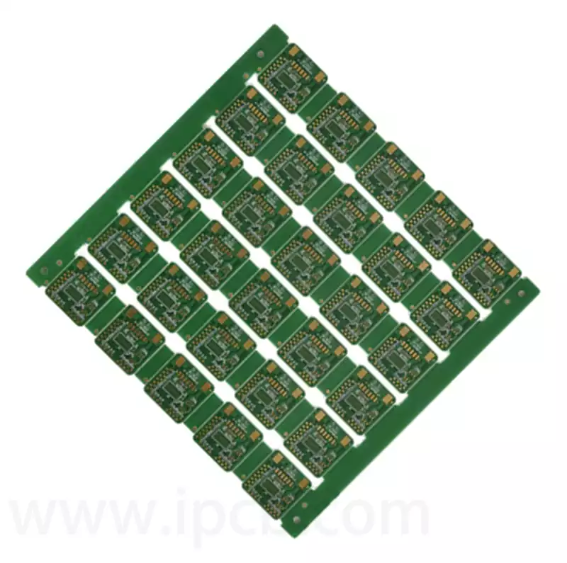
Glass substrates are regarded as crucial carrier plates for next-generation chip packaging, with glass serving as their core material. The key to realising glass substrate packaging lies in TGV technology. The entire glass substrate industry chain encompasses production, raw materials, equipment, process technology, packaging, testing, and end applications, with production, raw materials, and equipment constituting the upstream segment. Owing to their unique physical and chemical properties, glass substrates demonstrate broad application prospects within the electronic component materials sector.
What is Glass Substrate Chip Technology—TGV
TGV (Through Glass Via) technology, also known as glass through-hole technology, is a vertical electrical interconnection technique that traverses glass substrates. It enables the formation of vertical electrical connections on glass substrates, facilitating high-density interconnections between chips and between chips and substrates. While TSV (Through Silicon Via) technology penetrates the interposer layer on silicon interposer boards, TGV technology traverses the interposer layer on glass interposer boards. (Through Glass Via).
TGV technology evolved from 2.5D/3D integrated TSV interposer technology, with origins traceable to 2008. Its emergence primarily addressed issues in TSV interposers, including degradation of high-frequency or high-speed signal transmission characteristics due to silicon substrate loss, high material costs, and complex processes. Given the differing properties between glass and silicon/silicon dioxide materials, the key research focus became TGV interconnect technology involving through-hole etching and hole metallisation on glass substrates. Corresponding to silicon through-holes (TSV), TGV emerged as a potential new technology to replace silicon substrates.
Compared to silicon through-hole (TSV) processes, the advantages of glass through-holes (TGV) primarily lie in:
1) Superior high-frequency electrical properties. As an insulating material, glass possesses a dielectric constant approximately one-third that of silicon and a loss factor two to three orders of magnitude lower. This significantly reduces substrate loss and parasitic effects, ensuring signal integrity during transmission.
2) Large-format, ultra-thin glass substrates are readily available. Glass manufacturers such as Corning, Asahi, and SCHOTT supply ultra-large (>2m × 2m) and ultra-thin (<50µm) panel glass, alongside ultra-thin flexible glass materials.
3) Low cost. Benefiting from readily available large-size ultra-thin panel glass and the absence of insulation layer deposition, glass interposer fabrication costs are approximately one-eighth that of silicon-based interposers;
4) Simplified process flow. No insulation layer deposition is required on the substrate surface or TGV inner walls, and no thinning is needed in ultra-thin interposers;
5) High mechanical stability. Warpage remains minimal even when interposer thickness is below 100µm;
6) Broad application scope. As an emerging vertical interconnect technology for wafer-level packaging, it offers a novel technical pathway to achieve the shortest distances and smallest pitches between chips. Possessing excellent electrical, thermal, and mechanical properties, it holds unique advantages in fields such as RF chips, high-end MEMS sensors, and high-density system integration. It stands as one of the preferred choices for 3D packaging of next-generation 5G and 6G high-frequency chips.
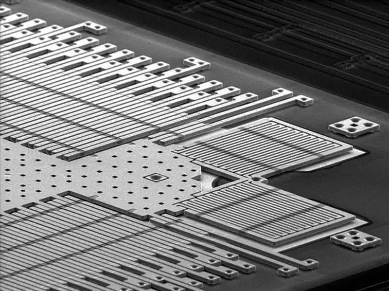
The TGV (Through Glass Via) glass substrate process flow aims to achieve three-dimensional integration by fabricating vertical interconnect vias. Its core steps comprise glass substrate preparation, via formation, via cleaning and surface treatment, metallisation, planarisation, and post-processing, as detailed below:
Glass Substrate Preparation: Select ultra-thin glass substrates with specific composition, thickness, and surface quality, ensuring high flatness, high cleanliness, and excellent thermal stability. Thoroughly clean using specialised equipment to remove surface contaminants such as dust and grease.
Via Formation:
Laser Drilling/Etching: Micro-holes are formed in the glass using femtosecond laser or wet/dry etching techniques. Laser drilling requires high-precision laser drilling equipment with strict control of laser parameters and drilling speed to ensure hole position, diameter, and shape meet design specifications. Holes are typically designed with a tapered shape to facilitate subsequent metallisation and electroplating filling.
Photolithography and Etching: Apply photoresist to the glass substrate surface. Using photolithography equipment, expose the designed via pattern onto the photoresist. The photoresist undergoes a chemical reaction in the exposed areas. Following development with a developer solution, the photoresist pattern corresponding to the via pattern is retained, serving as a mask for subsequent etching. The etching process may utilise dry etching (such as Reactive Ion Etching, RIE) or wet etching techniques, with precise control over parameters including time, temperature, and etchant concentration to ensure dimensional accuracy and shape quality of the vias.
Via Cleaning and Surface Treatment:
Cleaning:
Removes residual etchant, photoresist, and other contaminants from the etching process. Specific solvents are employed to remove photoresist, followed by multiple rinses with deionised water to ensure cleanliness within the vias and on the glass substrate surface.
Surface Activation:
Activates the glass surface and via walls through chemical solutions (e.g., containing silane coupling agents) to enhance adhesion between the subsequent metallisation layer and the glass substrate.
Metallisation:
Seed Layer Deposition: Employing Physical Vapour Deposition (PVD, e.g., sputtering) or Chemical Vapour Deposition (CVD), a thin metallic seed layer is deposited onto the glass substrate surface and via walls. Metals such as copper or titanium are typically selected. This seed layer serves as the conductive substrate for subsequent electroplating, providing an effective electrical pathway for metal filling.
Electroplating: Using the seed layer as the electrode, electroplating is performed in an electroplating solution. This causes the metal (e.g., copper) to grow and fill within the through-holes and on the glass substrate surface until the through-holes are completely filled, forming metal interconnect pillars with excellent conductivity. Electroplating parameters (such as current density, time, and temperature) must be controlled to ensure uniformity and quality of the metal fill.
Planarisation and Post-Processing:
Planarisation: Excess metal is removed from the glass substrate surface via processes such as chemical mechanical planarisation (CMP), achieving a smooth surface to guarantee planarity and electrical performance during subsequent interconnections with other devices.
Inspection and Testing: Optical microscopes and scanning electron microscopes (SEM) are employed to inspect via dimensions, morphology, and surface quality. Electrical testing equipment measures parameters such as via resistance and capacitance to verify TGV structures meet design specifications.
As a core technology for glass substrate packaging, TGV is forging novel development pathways for the semiconductor industry. Leveraging glass materials’ inherent advantages in dielectric properties, dimensional scalability, cost, and processability, TGV not only overcomes limitations of traditional silicon-based TSVs but also provides a new, reliable solution for advanced packaging requiring high-frequency, high-speed, high-density, and low-loss performance.
With the continuous maturation of materials, equipment, and processes, glass substrates and their TGV technology are poised for large-scale application in 5G/6G RF, advanced sensors, AI chips, and high-end packaging. They are set to become a pivotal supporting force in the future evolution of 3D packaging technology.