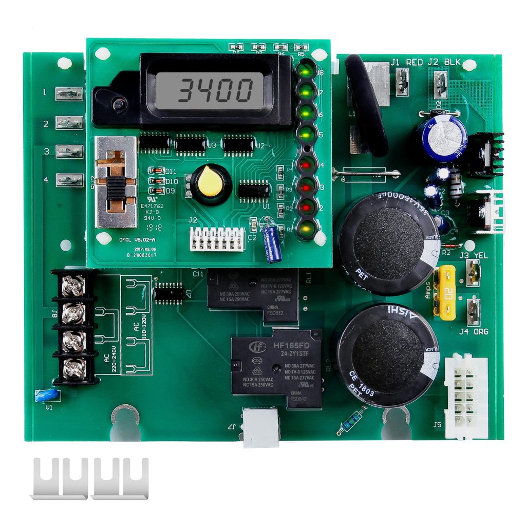
Definition of glx pcb main
glx pcb main is a main circuit board designed for the core of electronic devices. It is the central control unit of the system, responsible for managing and coordinating various functions and features. The motherboard is an integral part of electronic products such as computers, communication equipment, and home appliances, and Glx as a brand or company may focus on producing high-performance, high-quality PCB mainboards to meet the needs of different industries and products. The glx pcb main circuit board is a key component that allows users to control and monitor their pool or spa equipment, such as pumps, heaters, lights, and disinfection systems. It provides an interface between the user and the system, allowing for convenient programming, scheduling, and customization. If there are any problems or failures with the glx pcb main, always consult the manufacturer’s documentation or seek professional help for troubleshooting and repairs.
In the era of the electronics boom, chips and integrated circuits are the cornerstones. All electronic devices launched in the electronics revolution were not ready-made. Like the launch of any other product or device, it also goes through its own process, just like cooking a dish. In essence, in order to achieve electronic innovation, we need some basic utensils. Printed circuit boards play this role skillfully, ensuring the resonant purpose of performance and reliability. PCBs are key electronic components. In this article, we will discuss the detailed steps of PCB board manufacturing.
Electronic technology is moving towards integration technology day by day, which is known as scale integration, large-scale integration, very large-scale integration or popularly known as VLSI and very large-scale integration. While this technology has miniaturized our everyday devices like mobile phones, laptops or PCs and even TVs, it is amazing to take a look at the behind-the-scenes of this dramatic revolution. With the help of these integration technologies, our devices are getting smaller and smaller, but at the same time we need to mount the chips on small circuit boards as we know that chips are mounted on PCBs or printed circuit boards. Initially, circuit boards were made of physical wires and each conductive path was represented by an actual physical wire with different diameters depending on the purpose.
Today, our circuit boards have become so small in size that it is not appropriate to physically connect the tiny chips through jumpers or copper wires, and besides, it is almost impossible to take care of every line of the circuit accurately and precisely. Now, for the same reason, we use some software to design our circuit board layouts.
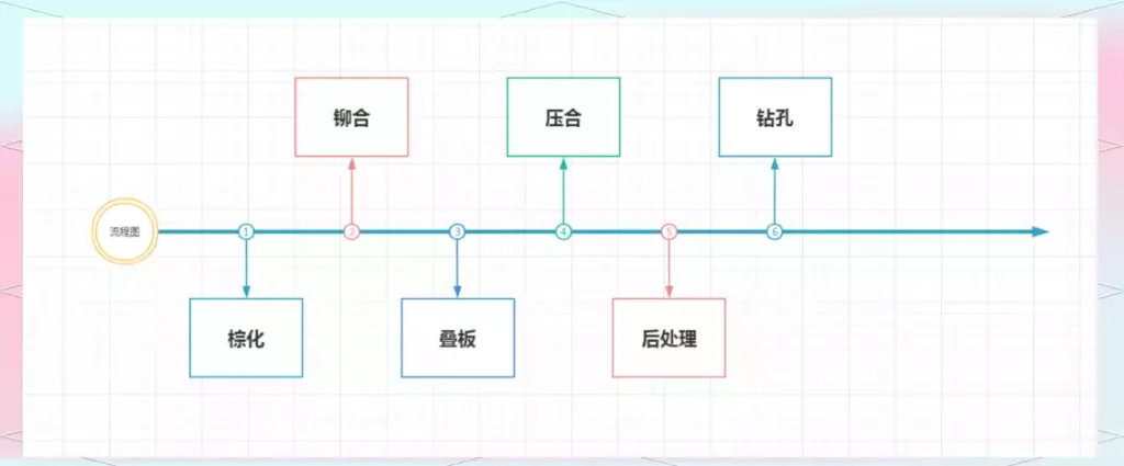
Steps of glx pcb board manufacturing:
To get a clear idea of the manufacturing process of PCB, let’s understand step by step how PCB develops from an idea on paper to the final product. When delving into the PCB manufacturing process, it is worth noting that PCBs come in many types and varying levels of complexity. The number of steps we need to complete is proportional to the complexity of the PCB board in question:
- PCB layout design:
Before any PCB board is manufactured, it needs to be laid out or designed. The layout of a PCB board is nothing but a circuit diagram in which each node has a clear path. The layout is not drawn with pen and paper, but with the help of software such as Altium Designer, OrCAD, Pads, KiCad, Eagle CAD, and EasyEDA. Using software not only saves time but also makes it easier to make any last-minute changes to the layout. Once the design is completed, it is converted into the appropriate format for use by the PCB board manufacturer. The most commonly used extension of PCB layout drawings is the extension Gerber file. Each Gerber file marks the design of a PCB board. The Gerber file is DFM checked (Design for Manufacturing) in the hands of the manufacturer to check if it meets all industry standards. After approval, the layout is printed. A special type of printer called a plotter is used to print the PCB layout. The plotter is not an ordinary inkjet printer, but a special type of laser printer. The PCB layout cannot be printed on ordinary A4 paper, but only on some special films.
When connecting two or more traces on a printed circuit board design, you should avoid forming a 90-degree angle because it makes the traces more susceptible to corrosion and scab on the board. The 90-degree angle is also more susceptible to radio frequency, which reduces stability. In contrast, it has been found and tested that a 45-degree angle ensures that we get the most traces on the minimum area on the PCB board and is not prone to corrosion. In addition to this, we may have seen parallel lines on the PCB board that are parallel to each other but of different lengths. This is called length matching of traces. As the name suggests, it matches the length of the path so that two or more signals arrive at a certain node at the same time and accurately, so that sometimes we need the signal to arrive at a specific point at a specific time.
- Substrate Cutting:
In this step, we cut the large sheet of PCB substrate into small pieces. For example, the substrate size is about 36×48 inches, and it is difficult to cut it into small pieces of 18×24 inches in PCB production. Its core consists of copper sheets and dielectric substrates. Epoxy resin (FR-4) is mainly used in multi-layer PCB board manufacturing, and fiberglass is used to make the board strong, durable and impact-resistant. Laminate is an ideal carrier for copper reception on both sides, also known as copper clad laminate (CCL). - Pattern Printing:
The PCB layout drawing is printed by a plotter on a negative film, which is marked with different ink areas. These negative films are also layer-specific, that is, for the inner layers of the PCB board, the black ink represents the conductive path and the other areas represent the non-conductive path. However, for the outer layers of the PCB board, the meaning of the ink color is completely different. In the outer layer, black represents the non-conductive path and the other areas mark the conductive path. - Photoresist Coating:
After cleaning, a layer of photoresist film is applied on the circuit board. The photoresist film consists of photoreactive chemicals that harden when exposed to UV light. The photoresist is applied in order to trace the conductive paths from the negative to the laminate with the help of UV light. A drilling machine is used to punch registration holes on all the holes to achieve perfect alignment of all the layers. After that, chemical copper is made through the board so that the PCB conductivity remains intact throughout the board and both the top and bottom surfaces remain connected. - Tracing Exposure:
In PCB construction, the most important process is the pattern tracing from the negative to the copper clad laminate. As mentioned earlier, different areas are traced on the film. When the copper clad laminate and its corresponding layout are stacked on it, some visible areas appear. These areas mark the conductive traces. When the UV light passes through, it passes through the visible area and reaches the UV-sensitive photoresist film and immediately melts and hardens on the copper clad laminate. Only the photochemically hardened part can be seen from the conductive traces of the film, and the rest is blocked by the black ink and remains semi-liquid. After all the paths are successfully traced, the board can be cleaned of the unwanted photoresist. To do this, it goes through an alkaline solution which cleans all the wet photoresist material on the PCB board and the hardened photoresist covers the conductive paths. - Etching of the outer copper layers:
The PCB board is almost ready and now the only thing that is not needed on it is the copper in the non-conductive areas. This process is called etching. To easily remove the excess copper, prepare a ferrous chloride solution in a 1:1 ratio and let the board soak in it for a few hours. The solution removes the copper from the board and only the copper covered with photoresist is left. To wash off the hardened photoresist, use acetone on the board and then water. - Alignment check:
To ensure that the locating holes are intact, a final check is required before all the layers are combined with each other. All the layers are placed inside a machine which uses the original Gerber file as a model to accurately check the location and alignment of the locating holes in all the layers. If no inaccuracies are found, the layers will enter the final stage of the PCB board manufacturing process; if inaccuracies are found, the inaccuracies will be displayed on the screen so that the manufacturer can fix them.
8.Lamination:
Generally speaking, in the process, we will laminate the inner copper layer with the outer copper layer, put dielectric material between the copper layers, and then heat press them to make them bond to each other. For example, when we purchase a four-layer printed circuit board, we will first make the core board (copper layers 2 and 3), and then put a thin layer of dielectric material (here we call it prepreg) and thin board on the top and bottom core boards, and then press them together through a press machine. - Drilling:
Now that a fully functional PCB board is ready, all layers are intact, and you can start drilling. Drilling is mainly used to connect all layers. Drilling is to solder components to the PCB board. Nowadays, most use surface mount devices (SMD), but this option is still retained. Holes are also punched to maintain the diversity of PCB uses.
10.Copper plating:
Copper plating has two functions: first, it is used to plate copper into the walls of the drilled holes to connect all copper layers; second, it will add thicker copper to the copper lines on the top and bottom layers. - Outer Layer Imaging and Etching:
During this process, the outer layers of the PCB board are traced in a similar manner to the inner layers. Once traced, the unwanted copper and other materials are also etched in a similar manner. A protective layer is applied to the newly formed boards to protect them from further etching processes where the desired conductive paths may get damaged and may cause the board to malfunction. After all etching processes are completed, it is then removed chemically. - Solder Mask:
It is usually the green mask we see on printed circuit boards. The solder mask is applied on the surface of the PCB to prevent oxidation and corrosion damage and to isolate it from other circuits during the PCB assembly process. - Silk Screen:
Finally, if there are any labels or icons in the layout design that need to be printed on the PCB board, this can be done through silk screen printing (inkjet printing). Silk screen printing is used for information graphics on PCB boards. - Surface Finish:
It is a layer of tin solder or immersion silver, gold plating or other metals applied to the PCB board. This is done to provide the circuit board with extra protection against dust, moisture and oxidation, and also facilitates PCB assembly. - Electrical Testing:
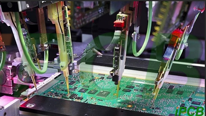
Before releasing the circuit board to the market, all circuit boards are first electrically tested, and some manufacturers sometimes provide some special tools to perform the tests. If the test results are suitable, the circuit board is released to the market for innovators, engineers and all those who need it. - Final Inspection:
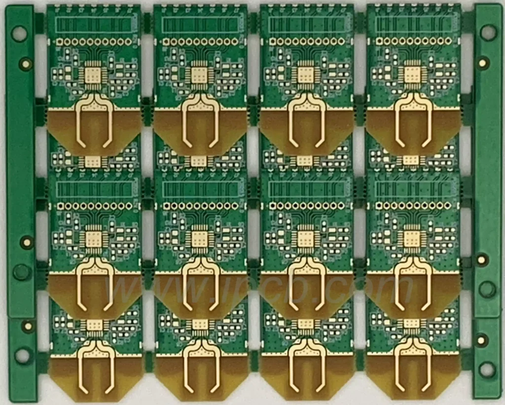
After the testing is completed, the production of the PCB board is basically completed. But before shipping, we still need to check for minor visual defects such as scratches through inspection machines or manually.
That’s all about PCB board manufacturing. But we have to consider that this is just the standard process for multi-layer circuit boards. There are some major differences between the processes of multi-layer circuit boards. Double-layer (or single-layer) PCB and multi-layer PCB. In double-layer PCB boards, there are copper cladding or copper vias on both sides, but in multi-layer boards, we have multiple copper layers stacked on top of each other, so double-layer PCBs do not require lamination. In multi-layer PCB boards, complex designs may require blind and buried vias.
Core Features of Glx PCB Motherboard
High-precision design: glx pcb main usually adopt high-precision design and manufacturing processes to ensure that the circuits on the motherboard can work stably and reliably, especially in high-speed signal transmission and high-power applications.
Multi-layer structure: Most glx pcb main are multi-layer board designs with multi-layer circuits, which can provide higher circuit density, better performance, and more complex functions, which makes them suitable for devices that require high integration.
Good heat dissipation performance: Electronic devices generate heat during operation, especially high-performance motherboards. glx pcb mains usually use high-quality materials and design solutions to ensure that the motherboard has good heat dissipation performance, thereby maintaining the stable operation of the device.
Highly integrated: In modern electronic devices, glx pcb main need to support the integration of multiple functions, such as processors, memory, graphics cards, network connections, etc. They are designed with high-density integration in mind and can complete complex circuit layouts in a limited space.
As the core component of electronic equipment, glx pcb main have a wide range of applications in many fields such as computers, consumer electronics, industrial automation, and automotive electronics due to their high integration, stability, and reliability. With the advancement of science and technology and the changes in market demand, the technology and manufacturing process of glx pcb mains will continue to innovate and improve, helping to realize various intelligent products and systems. In the future, with the continuous development of electronic technology, glx pcb mains are expected to play an important role in more high-tech fields.