Gold plated circuit board is a special type of circuit board plated with a layer of gold on the surface of the circuit board’s pads. The principle is that the nickel and gold (commonly known as gold salt) dissolved in a chemical solution, the circuit board will be immersed in the plating cylinder and turn on the current in the circuit board on the surface of the copper foil to generate nickel-gold plating, nickel-gold plating due to the high hardness of the plating layer, wear-resistant, not easy to oxidize the advantages of the electronic products in a wide range of applications.
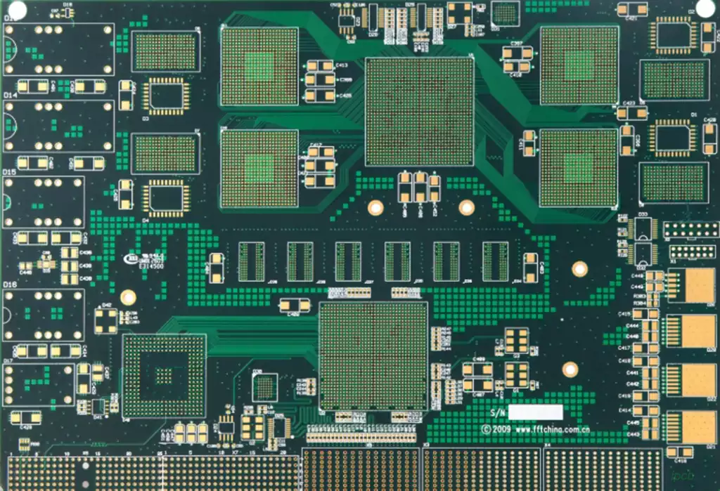
Gold plated circuit boards are mainly used in high-precision, high-reliability electronic products, such as aerospace, medical equipment, military equipment, communications equipment, industrial control equipment. They have high stability and reliability in circuit connection and signal transmission and also have better performance in high frequency and microwave environments. In addition, gold-plated circuit boards are also commonly used in consumer electronics such as high-end cell phones, tablets, and laptops to meet increasing performance and functionality requirements.
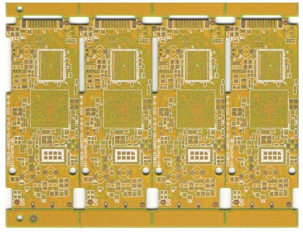
Gold plating itself can be divided into hard gold and soft gold. Because hard gold plating is actually an alloy plating (that is, plated with Au and other metals), so the hardness will be more hard, suitable for use in the need for force and friction, in the electronics industry is generally used as a circuit board board edge contact (commonly known as the “Gold Finger” place, such as shown in the picture at the top). Soft gold is generally used for COB (Chip On Board) above the aluminum wire, or cell phone button contact surface, and recently has been used in a large number of BGA carrier board front and back.
The purpose of electroplating is basically to be “gold” plated on the copper skin of the circuit board, but “gold” and “copper” in direct contact, there will be electron migration diffusion of the physical reaction (potential difference relationship), so it must be plated as a layer of “nickel” as a barrier layer, and then plated to the top of the nickel gold, so what we generally call gold plating, the actual name of the nickel plating should be called “gold plating”.
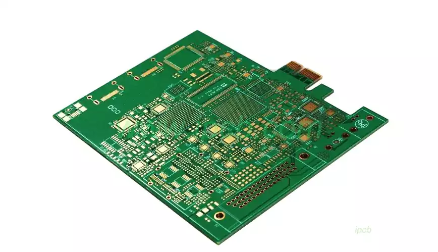
In some small-sized PCBs, gold plated circuit boards can reduce costs. Compared with the traditional electroless nickel-gold process, gold-plated circuit boards require shorter plating times and thinner gold-plating layers, which reduces production costs.
Gold plated circuit boards offer the following advantages:
Enhanced electrical conductivity: It can significantly improve the electrical conductivity of electronic equipment, ensuring that the electronic equipment has good electrical performance during operation.
Prevent oxidation: the surface is covered with a layer of metallic gold, which can prevent the circuit board surface oxidation corrosion, prolonging the service life of electronic equipment.
Aesthetically pleasing: smooth, delicate surfaces, and bright colors, can increase the aesthetic appearance of electronic equipment, and improve the added value of the product.
Easy to maintain: smooth surface, not easy to adhere to dust and dirt, can be easily cleaned and maintained.
Environmental protection: Recycling gold-plated circuit boards is an important environmental protection action because the hazardous substances in electronic waste can cause great harm to the environment and human health. Recycling these pcb boards not only reduces the waste of natural resources but also reduces the pollution of the environment.
However,it also has some drawbacks, such as higher cost and poor solder strength. Nevertheless, due to its excellent performance and wide range of applications, it has become an important part of the electronics industry.
Appearance standards of PCB gold plating
High-quality gold plated circuit board should meet the following appearance standards:
Uniform color: the gold layer should present a consistent golden yellow color, without obvious color difference or spots.
Smooth surface: the gold-plated surface should be smooth and flawless, without pinholes, cracks or bumps.
Moderate thickness: according to the application requirements, the thickness of the gold plating layer should be within the specified range, too thick may affect the welding, too thin will affect the corrosion resistance.
Complete coverage: All copper surfaces to be protected should be completely covered by the gold layer, with no exposed copper traces.
Solderability: The gold-plated surface should maintain good solderability to meet the subsequent assembly requirements.
Gold plated circuit board is gradually becoming the new focus of the electronics industry due to their excellent performance and aesthetic appearance. With the progress of science and technology and the continuous expansion of application areas, we believe that the gold-plated circuit boards will play a greater potential in the future, to bring more innovation and breakthroughs in electronic products.