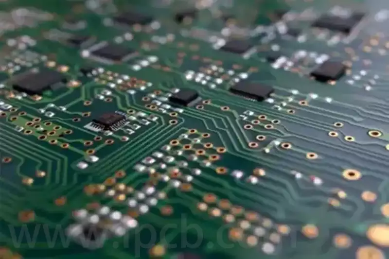
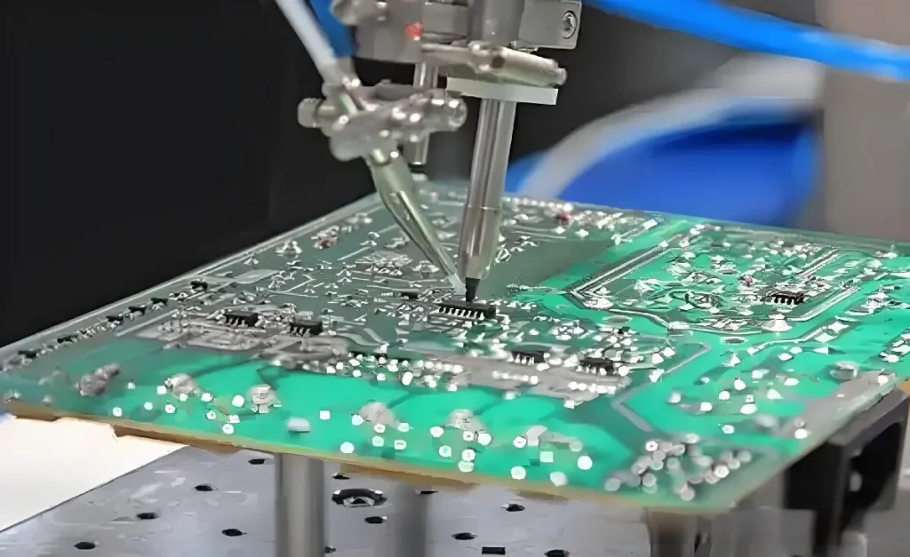
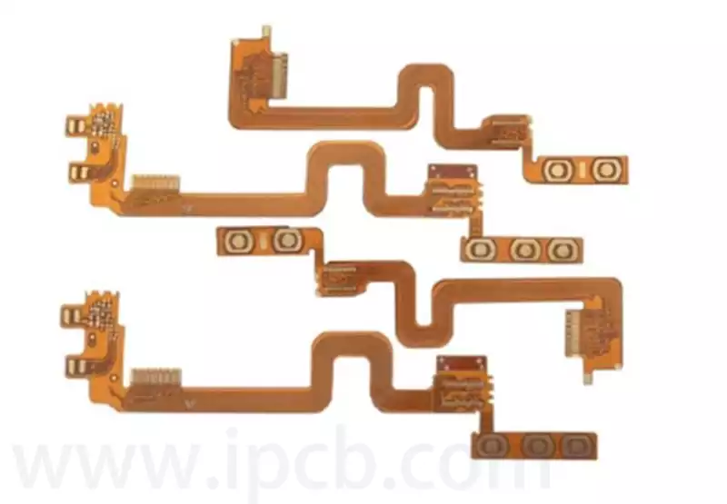
In today’s high-tech industry PCB, HDI PCBs have become a core element in the manufacture of electronic devices. They play a vital role in a variety of applications, including communications, medical devices, aerospace, consumer electronics, etc. The outstanding performance, reliability, and stability of HDI PCBs make them key to meeting the demands of modern devices. In this paper, we will introduce the HDI board design in detail, as well as in practice to optimize the performance and efficiency of the strategy.
1.Overview of HDI Printed Circuit Boards
It is an advanced circuit board technology, it is through the high-density interconnect (HDI) technology to achieve smaller, lighter, more reliable circuit board design. HDI PCB has thin, miniaturized, and high-density features to support high-speed, high-frequency signal transmission.
2. HDI circuit board design process
Demand analysis: clear design requirements, including board size, number of layers, wiring density, and material selection. Ensure a full understanding of customer needs, laying the foundation for subsequent design.
Design Preparation: Select the appropriate HDI PCB design software, and pre-design preparatory work, such as setting units, parameters, etc..Choosing the right design software is crucial to improving design efficiency and accuracy.
Schematic Design: Use circuit design software to create a circuit schematic to ensure that the circuit functions correctly. In the schematic design, focus on component selection and circuit layout to lay the foundation for subsequent PCB design.
PCB Layout: In the HDI PCB design software, a reasonable layout design is carried out according to the requirements, taking into account the wiring, component spacing, component placement, and other elements. The layout needs to follow certain rules and techniques, such as avoiding cross-wire, rational use of space, and so on.
PCB wiring: based on the layout of the wiring design, follow the wiring rules to ensure the quality of signal transmission. The wiring process should focus on line width, spacing, and corner control, as well as consider the signal flow shielding and other issues.
DFM Review: Conduct a Design for Manufacturability review to ensure that the design meets manufacturing requirements. This step is critical to identify and correct manufacturing limitations and potential problems in the design.
Design Export: Export design files, including Gerber files, drill files, etc., for subsequent manufacturing. Ensure that the file format and parameter settings comply with manufacturing requirements to ensure a smooth manufacturing process.
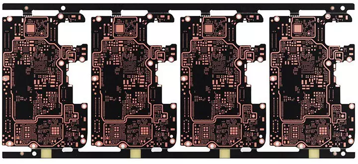
3. HDI printed circuit board optimization strategy
Layout optimization
Component arrangement: Try to arrange components of the same function or type together to improve the regularity and maintainability of the layout.
Signal flow planning: According to the signal transmission direction and characteristics, rational planning of components and wiring arrangement direction, improve the signal transmission efficiency and stability.Power supply/grounding design: Reasonable planning of power supply and grounding network to reduce power supply noise and signal interference. Adopt a multi-layer board structure to improve the reliability of the power supply and grounding layer.
Cabling optimization
Selection of appropriate line width and spacing: According to the signal transmission rate and electrical performance requirements, select the appropriate line width and spacing to ensure stable signal transmission. Optimize wiring paths: Use straight lines, arcs, and other continuous and smooth paths for wiring, reduce the line’s transitions and intersections, and reduce signal reflection and interference.
Consider Electromagnetic Compatibility (EMC): Incorporate appropriate shielding and isolation measures in wiring to reduce electromagnetic interference and signal leakage.
Multilayer HDI board design
Utilize multilayer board structure: multilayer board design can increase wiring space and improve signal density. A reasonable setup of inner layer connections and power/ground layers can improve circuit performance and stability.
Optimizing interlayer connections: Properly planning the location and number of interlayer connection holes ensures reliable signal transmission and reduces manufacturing costs.
Buried and blind vias
Utilizing buried and blind vias: these techniques can reduce surface wiring and improve wiring density and reliability. The performance of HDI PCBs can be further optimized by planning the location, number, and timing of buried and blind vias.
Material Selection: Selection of suitable substrate material: Select the suitable substrate material according to the application requirements, such as FR4, CEM-1, or polyimide. Consider the electrical, mechanical, and reliability requirements of the material.
Selection of high thermal conductivity materials: For high power and high heat generation components, select materials with good thermal conductivity to improve heat dissipation performance.
Reliability testing and simulation
Conduct simulation tests: Use simulation software to test and verify signal integrity, power integrity, and electromagnetic compatibility. Evaluate the reliability and performance of the design through simulation testing.
Conduct reliability tests: Conduct reliability tests such as environmental adaptability tests, vibration tests, etc., before actual HDI PCB manufacturing.
