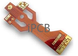
What is hdi pcb?hdi pcb board, i.e. high density interconnect circuit board, is a new type of circuit board that adopts precision manufacturing technology and materials to realize high integration and high reliability of the circuit board. It adopts microvia technology, through laser drilling or mechanical drilling, to form tiny through holes on the board, thus realizing the interlayer interconnection of the board. Compared to traditional pcb boards, it has higher wiring density, finer lines and smaller apertures, enabling more complex circuit designs to be realized in a limited space.
HDI circuit board production process mainly includes the following steps:
- Design: first, according to the schematic diagram of the circuit, the design of the circuit board.
- Plate making: Use the relevant software to integrate the designed circuit board diagram into a Gerber file, and make the plate on the substrate of the circuit board with the light board.
- Inner layer manufacturing: The circuit diagram made by the optical board is molded on the substrate to form the desired line.
- Film formation: Chemical copper plating or copper plating on the surface of the PCB to form a copper foil layer.
- Laser Drilling: Drill holes in the copper foil layer with a laser.
- Outer layer manufacturing: The board is pressed onto the chemically coated copper foil layer to form the outer circuit.
- Windowing: Through photolithography and etching processes, the outer circuit board is windowed for soldering components.
- Surface treatment: the finished circuit board is chemically treated to turn its surface into solder alloy and other things.
- Antirust treatment: spraying and other antirust treatment of the circuit board to improve its service life.
After completing all the above steps, you can make a high-quality HDI pcb board.
HDI circuit boards are very difficult to produce and require strict site management and operating procedures. Only through strict quality management and quality control can the high reliability and stability of the circuit board be guaranteed.
Difference between hdi circuit board and ordinary pcb.
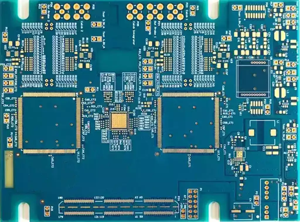
Wiring density: hdi board wiring density can realize more signal lines in a very small size, providing more complex circuit design.
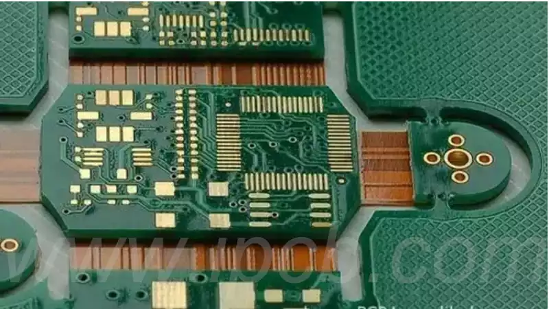
Multi-layer structure: hdi board with 4 layers and more than 4 layers of multi-layer structure, can provide a lot of signal layer, power layer and ground layer, to support complex signal transmission and circuit connection
Size: hdi boards are characterized by high-density wiring and multi-layer structure, with this advantage hdi printed circuit boards are able to make smaller sizes, making them more suitable for compact packages and space-constrained applications.
Manufacturing process: hdi boards use laser drilling and light painting technology and other high-precision process control and advanced manufacturing equipment to ensure the accuracy of the hole position and detailed line pattern.
Electrical properties: hdi board has very good electrical properties, enhanced signal strength and improved reliability, improved RF interference, electromagnetic wave interference, electrostatic discharge, heat conduction and other aspects.
Requirements for buried holes and plug holes: hdi board production and manufacturing of difficult to bury holes and plug holes in the requirements are very high, so hdi board compared to ordinary pcb manufacturing threshold and process to be more difficult.
Performance and application areas
Because HDI board has high density, high precision and high reliability and other characteristics, so in the performance and application areas and ordinary PCB there are obvious differences:
Signal transmission performance: HDI boards have better signal transmission performance due to higher wiring density and shorter signal transmission paths. This makes HDI boards have a significant advantage in high-speed, high-frequency and other application scenarios.
Heat dissipation performance: The design of HDI board makes its heat dissipation performance relatively poor, while ordinary PCB has relatively good heat dissipation performance due to its lower wiring density and larger heat dissipation area.
Application areas: HDI boards are mainly used in high-end electronic products, such as smart phones, tablet PCs, high-performance computers and so on. While ordinary PCBs are widely used in a variety of electronic devices, from home appliances to industrial control equipment.
Cost and Price
Due to the higher complexity of HDI boards in terms of design and manufacturing, as well as the higher cost of materials and equipment used, their price is usually higher than that of ordinary PCBs.This makes ordinary PCBs potentially more competitive in cost-sensitive application scenarios.
Advantages of hdi printed circuit boards
High Integration: The use of micro-blind/buried hole technology enables more circuit connections to be realized in a limited space, thus increasing the integration of the board. This means that electronic products can realize more functions while maintaining a compact size.
High performance: The use of finer wiring and smaller apertures helps to reduce signal loss and noise interference on the board, improving its performance. At the same time, high integration also means tighter connections between components on the board, helping to reduce latency and increase data transfer speeds.
High reliability: A variety of sophisticated and advanced technologies and materials are used in the manufacturing process, such as copper layer thickening and conductive material optimization, thus improving the reliability and stability of the circuit board. In addition, the micro-blind buried hole technology also helps to reduce defects and failure points on the boards and improve product yields.
With its superior high-density interconnect technology, HDI PCB not only meet the demand for high performance and high reliability of electronic products, but also promote the continuous development of the circuit board manufacturing industry.