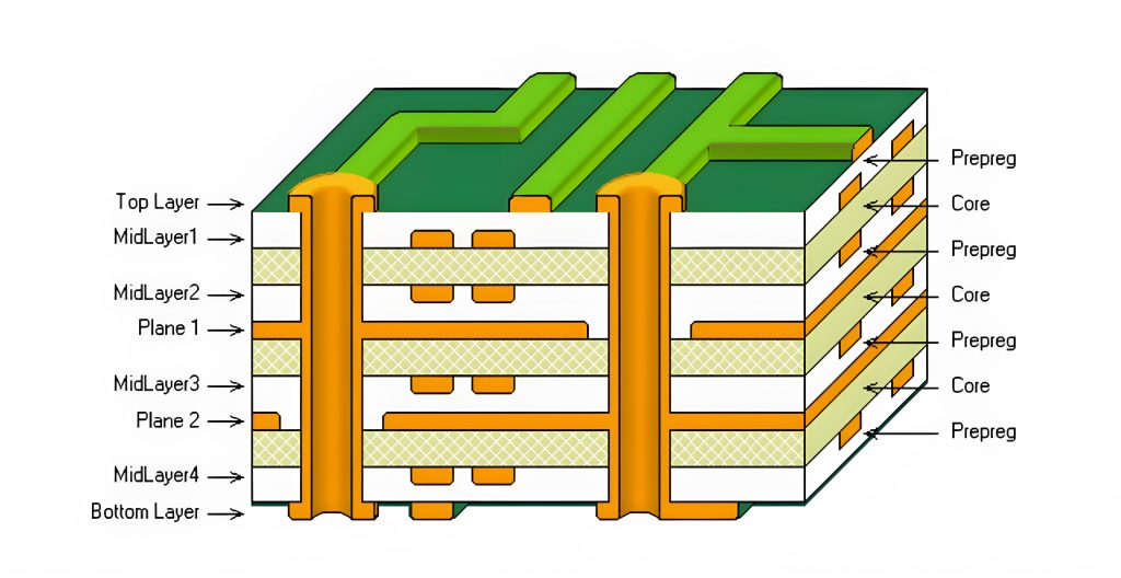
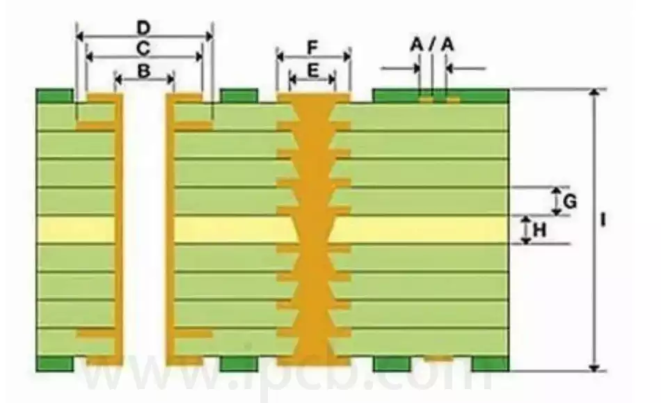
HDI PCB is usually manufactured using the stackup method, the so-called ‘stackup’ refers to the formation of complex multilayer structures through the stacking and compression of multiple layers of circuit board materials. The more layers are stacked, the more difficult the board’s performance and process will be. HDI pcb stackup structure is usually expressed in a layered manner, such as ‘1+4+1’, ‘1+1+4+1+1’, etc., and these numbers represent the number of layers and their distribution, reflecting the entire board. These numbers represent the number of layers of each board and their distribution, reflecting the internal structure of the board and connection.
Common hdi pcb stackup structures:
Basic Primary Layer Printed Boards
Example structure: (1+4+1)
Description: This structure represents the starting point of an HDI design and consists of an upper and lower layer (usually signal or power/ground), with an inner signal layer in the middle four layers, and is suitable for applications with medium wiring density.
Conventional Layer-at-a-time HDI PCB
Structure example: (1+4+1)
Description: Similar to the basic Primary Layer Accumulation, but this model focuses on HDI technology, using microvia technology to optimise line connections, thus improving wiring density and signal quality.
Conventional Secondary Layers HDI PCB
Structure example: (1+1+4+1+1)
Description: More layers and more complex interconnection structures are realised through the twice-layered technology, suitable for high-end electronic products.
Variant Two-Time Layer Building HDI PCB
Structure example: (1+1+2+1+1)
Description: Relatively fewer layers, but with unique layout and wiring design to meet specific application requirements such as controlling cost or achieving special performance.
Secondary Accumulation Layer HDI with Blind and Buried Vias Combined
Structure example: (1+1+4+1+1) featuring blind vias stacked above buried vias (layers 2-7)
Description: This design combines blind and buried vias to provide a more flexible interlayer connection solution, which effectively improves cabling efficiency and signal transmission performance.
Cross-layer Blind Vias Secondary Layers HDI PCB
Example structure: (1+1+4+1+1), with a focus on cross-layer blind vias
Description: Cross-layer blind vias allow signals to connect directly to different layers without having to pass through all intermediate layers, significantly improving wiring efficiency and signal integrity.
Reasonable hdi pcb stacKup layer design is the key to achieving high-performance, highly integrated hdi pcb, directly affecting the high-speed transmission of signals, impedance control and electromagnetic compatibility (EMC) and other performance indicators. With the development of electronic products to miniaturisation and high-speed, HDI technology is constantly upgraded, and high-order multi-layer and arbitrary-order stacked layer structures have emerged to meet the increasingly complex design requirements. In addition, the optimisation of the stacked layer structure can also significantly improve production efficiency and reduce manufacturing costs. For example, by optimising the layout of blind and buried holes and reducing the number of press-fits, it is possible to shorten the manufacturing cycle while maintaining performance and enhancing market competitiveness.