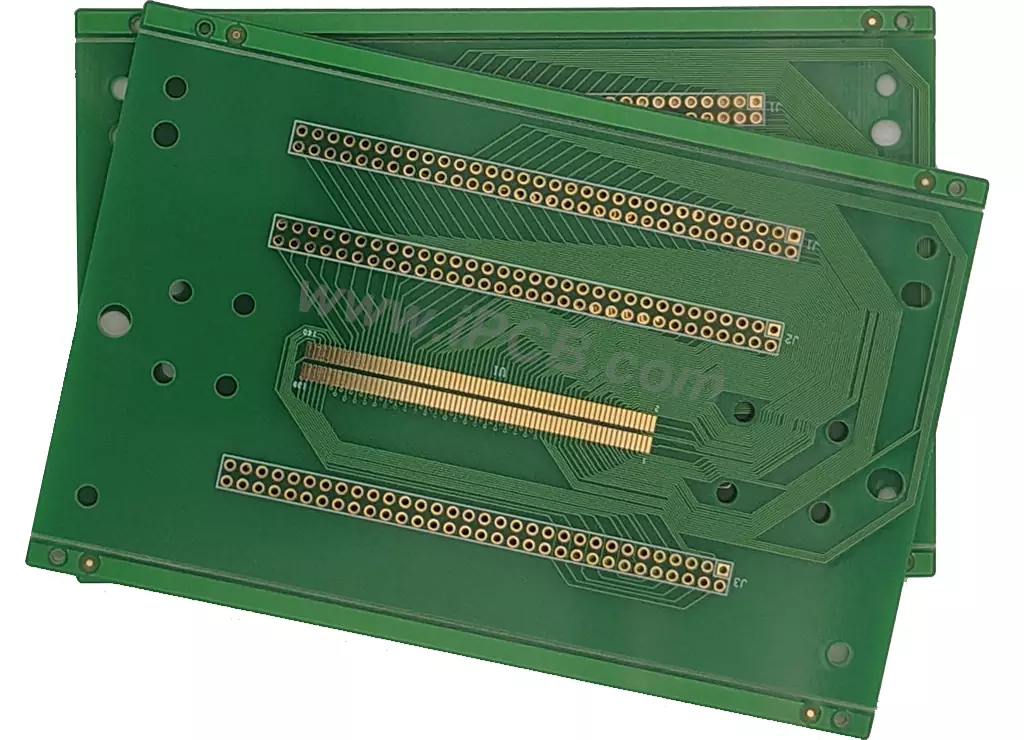
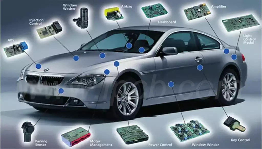
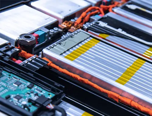
HDI technology is a cutting-edge PCB (Printed Circuit Board) manufacturing process that offers the significant benefits of high-density layout, high reliability and high integration, with the PCB serving as the cornerstone of electronic component interconnectivity, carrying and solidly connecting all types of electronic assemblies. Through the application of high-density integration HDI technology, can promote the miniaturisation of end-product design, and to meet the ever-increasing performance and efficiency standards of electronic products.
https://ipcb.co/hdi-pcb/The core advantages of HDI technology:
1.Tight integration of lines and components: HDI technology with the help of micro-blind holes, buried holes and other subtle structures, to achieve a tight integration of lines and components, significantly reducing the footprint of the PCB board, which in turn promotes the thin and light process of the product.
2.Excellent electrical characteristics: HDI technology uses laser drilling, plating and filling holes and other exquisite technology to ensure the solidity of the connection between the lines and excellent electrical conductivity, thus enhancing the reliability and stability of the product.
3.Efficient production process: HDI technology integrates automated production lines and advanced PCB manufacturing equipment to achieve a high degree of automation and informationisation of the production process, which strongly promotes the double improvement of production efficiency and quality.
4.In line with the concept of environmental protection: HDI technology adopts environmentally friendly materials and processes, effectively reducing the negative impact on the environment, in line with the current trend of green environmental protection.
The widespread adoption of HDI technology on the PCB (Printed Circuit Board) industry has brought about profound changes, its impact is mainly reflected in the following aspects:
1.Technical innovation and upgrading: With the popularity of HDI technology, the PCB industry ushered in the technical level of innovation and upgrading. In order to meet the market’s urgent demand for high-density, high-reliability and highly integrated products, PCB manufacturers have introduced cutting-edge production equipment and technology, in order to enhance their own technical strength and production capacity.
2.Product creativity and diversification: the popularity of HDI technology for the PCB industry product innovation has injected new vitality. With this technology, PCB manufacturers can develop more innovative, creative products to meet the market and customers increasingly diverse needs. For example, flexible PCB boards, PCB boards designed for wearable devices and other new products continue to emerge, enriching the market choice.
3.Changes in the pattern of market competition: the popularity of HDI technology has further intensified market competition in the PCB industry. In order to maintain a leading position in the fierce market competition, PCB manufacturers have to continue to improve product quality and service levels, while trying to reduce production costs and prices. This competitive situation promotes the continuous progress and development of the industry.
4.Enhancement of environmental awareness and green production: the popularity of HDI technology has also increased the PCB industry’s attention to environmental requirements. In order to meet the strict provisions of environmental regulations and customer demand for environmentally friendly products, PCB manufacturers have to use environmentally friendly materials and processes for production, promoting the industry to green, sustainable direction.
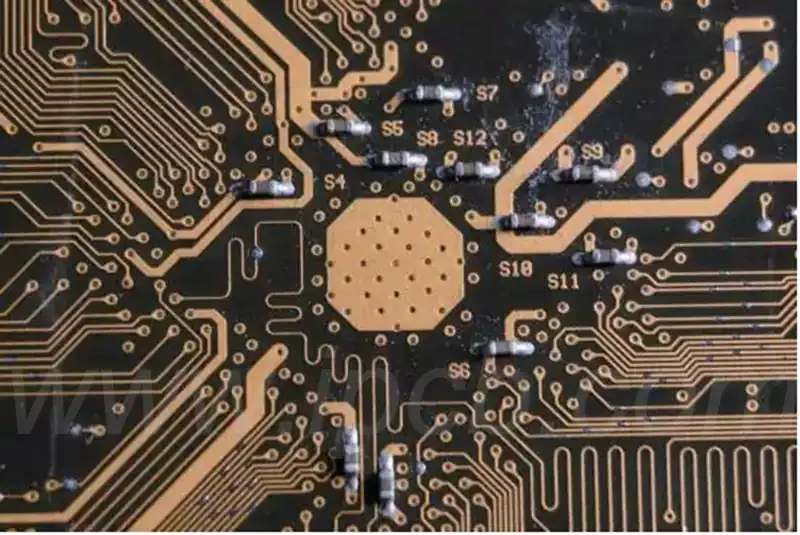
Looking ahead, the development trend of HDI technology in the PCB industry:
1.Technological innovation and upgrading: With the rapid changes in technology, HDI technology will continue to usher in innovation and breakthroughs. This includes the realisation of smaller apertures, the construction of more layers of circuit boards, the engraving of finer lines, as well as the development of advanced features such as low loss, high glass transition temperature (High Tg), low coefficient of thermal expansion (Low CTE), etc., which will jointly promote HDI boards to a higher stage of development.
2.Broadening of application areas: With the booming development of 5G communications, Internet of Things (IoT), artificial intelligence (AI) and other cutting-edge technologies and the continuous extension of application boundaries, the application scenarios of HDI technology will become increasingly rich. Especially in cutting-edge fields such as smart home and smart medical care, HDI technology will show more application potential and bring revolutionary solutions to these industries.
3.Green and sustainable development: With the general awareness of environmental protection and the increasingly strict laws and regulations, green and sustainable development has become an irreversible trend in the PCB industry. The use of environmentally friendly materials and production processes for production will not only become a mainstream practice in the industry, but will also be widely recognised and promoted, leading the PCB industry towards a greener and more sustainable future.
HDI PCB design process covers a series of vital links, as follows:
- Demand clear: At the beginning of the design, in-depth exchanges with customers, clear product features, performance standards, size constraints, etc., to lay the parameter basis for HDI PCB design.
- Preliminary conception: Based on the demand analysis, the designer proceeds with the preliminary design, covering the circuit layout, component screening and preliminary line planning.
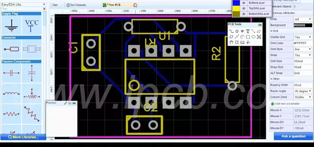
- Schematic drawing: using professional PCB design software, such as Altium Designer, Cadence or Eagle, carefully draw the circuit schematic to ensure that the circuit logic is accurate.
- Layout planning: After the completion of the schematic, enter the PCB layout stage. This link needs to take into account the signal integrity, electromagnetic compatibility (EMC), thermal management and other factors, and into the HDI-specific design elements, such as microvias, blind holes and buried holes in the application.
- Line design: After the layout is determined, fine line design, HDI PCB line design needs to be highly sophisticated to adapt to the dense component layout. Designers need to use multi-layer lines and microstrip line technology to optimise signal transmission.
- Thermal management design: For high power or high heat components, thermal management design is implemented to ensure that the PCB does not overheat during operation. This may involve the design of heat sinks, heat pipes or fans.
- Signal Integrity Verification: Use simulation tools to perform signal integrity analysis to ensure that high-speed signal transmission remains clear and interference-free.
- Electromagnetic compatibility assessment: electromagnetic compatibility analysis to ensure that the PCB design does not cause interference to other equipment, nor affected by other equipment.
- Prototype development: After the design is finalised, the PCB prototype is produced. This usually requires close co-operation with the PCB manufacturer to select the appropriate materials, processes and test methods.
- Testing and validation: After the prototype is made, a full range of tests are carried out, covering functionality, performance and reliability tests, to ensure that the PCB meets the design requirements.
- Design optimisation: According to the test results, make necessary adjustments and optimisation to the design to solve potential problems.
- Design finalisation: After several iterations, the design is finally confirmed and ready for mass production.
- Production Preparation: Collaborate with the manufacturer to prepare the materials, tools and processes required for production.
- Mass Production: Start mass production of HDI PCBs and implement strict quality control to ensure that each PCB meets the design specifications.
- Post-processing: After production is completed, surface treatment, component assembly and other post-processing.
- Final Test: After assembly, comprehensive testing is conducted to ensure that the performance and reliability of the entire product meets the standards.
HDI technology with its high-density layout, high reliability and high integration and other significant advantages, is profoundly changing the face of the PCB industry. From promoting technological innovation and upgrading, stimulating product innovation vitality, to intensify market competition and enhance environmental awareness, the popularity of HDI technology undoubtedly for the PCB industry has injected new vitality.
