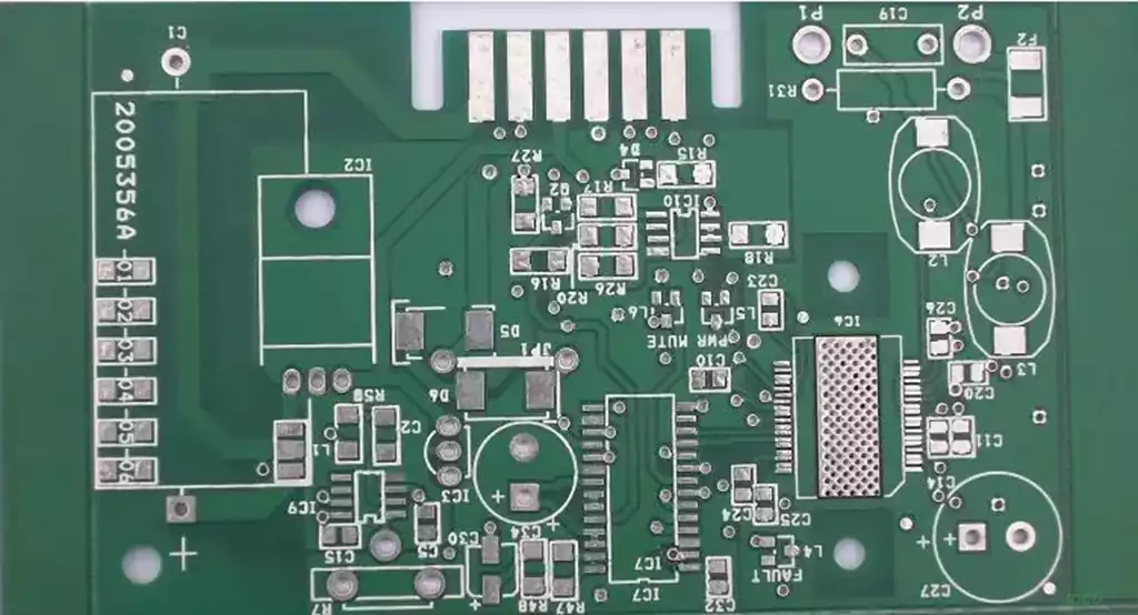
HF board refers to special circuit boards with high electromagnetic frequency, which are used in the field of high frequency (frequency greater than 300MHZ or wavelength less than 1 metre) and microwave (frequency greater than 3GHZ or wavelength less than 0.1 metre), and the circuit boards are produced by using some of the processes of the ordinary rigid circuit board manufacturing methods or by adopting the special treatment methods on copper-clad laminated boards of the microwave substrates. Generally speaking, high-frequency board can be defined as the frequency of 1GHz or more circuit boards.
HF board features
1.Signal integrity: due to the high operating frequency, the signal in the transmission process will occur reflection, attenuation, delay and other phenomena, resulting in signal distortion. Therefore, high-frequency and high-speed PCB circuit boards need to take a series of measures to ensure signal integrity, such as impedance matching, differential signal transmission, ground and power line layout.
2.Material Characteristics: High-frequency, high-speed PCBs require the use of low dielectric constant and low-loss materials, such as polytetrafluoroethylene (PTFE), ROGERS, etc., in order to reduce signal transmission losses and delays. Stacked Layer Design: Stacked layer design is one of the keys to high frequency and high speed PCB circuit board design. Reasonable stacked layer design can reduce signal transmission interference and crosstalk, improve the performance of the circuit board.
3.Manufacturing process: high-frequency PCB circuit board manufacturing process requirements, the need to use high-precision processing equipment and strict process control to ensure the quality and performance of the circuit board.
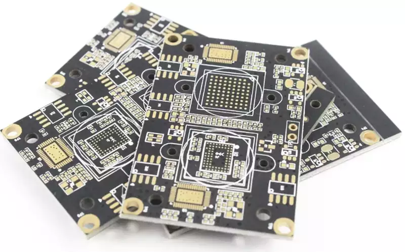
HF board material classification
A.Material points:
a.Organic materials: phenolic resin, glass fibre / epoxy resin, Polyimide, BT / Epoxy and so on belong to.
b.Inorganic materials: aluminium, Copper-invar-copper, ceramic and so on. Mainly for its heat dissipation function.
B.Distinguish between hard and soft products
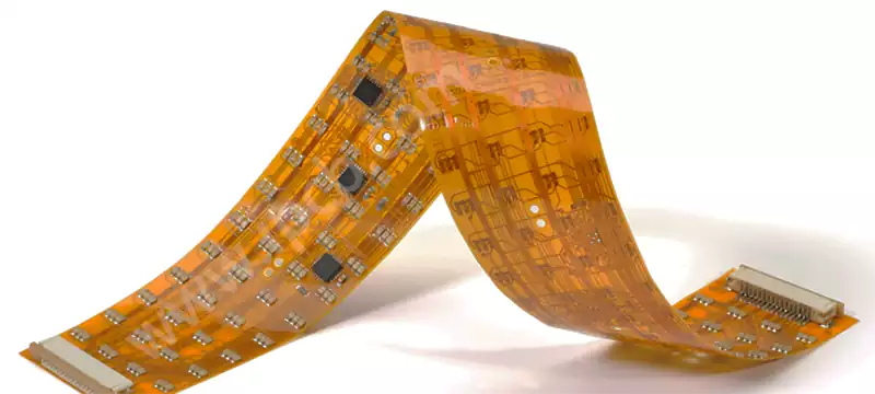
a.Rigid PCB, b. Flexible PCB, c. Rigid-Flex PCB
b.TUC: Tuc862, 872SLK, 883, 933, etc.
C.Structure
a.Single-side board, b. Double-side board, c. Multi-layer boards
D.According to the use of points
Communication/consumable electronics/military/computer/semiconductor/electrical board…
Selection of HF board materials what are the important indicators
When selecting a substrate for PCBs used in high-frequency circuits, it is important to examine in particular the characteristics of the material DK, which changes at different frequencies. For the focus on high-speed signal transmission requirements, or characteristic impedance control requirements, focus on DF and its performance in frequency, temperature and humidity and other conditions.
The general type of substrate materials in the frequency change conditions, showing a large change in the DK, DF value of the law. Especially in the frequency of l MHz to l GHz, their DK, DF value changes are more obvious. For example, the general type epoxy resin a glass fibre cloth-based substrate material (general type FR-4) in the frequency of l MHz under the DK value of 4.7, while in the frequency of l GHz under the DK value of 4.19. More than l GHz, the change in its DK value tends to be flat. The trend of change is with the increase in frequency, and become smaller (but the magnitude of change is not large), for example, in l0GHz, the general FR a 4 DK value of 4.15, with high-speed, high-frequency characteristics of the substrate material in the case of frequency change, the DK value of the change in the smaller, since the l MHz to lGHz changes in frequency, the DK more than to remain in the 0.02 range of changes. Its DK value in different frequency conditions from low to high, a slight tendency to decline.
General type substrate material dielectric loss factor (DF), in by frequency change (especially in the high frequency range of change) and produce DF value change than DK.The rule of change is tending to increase, therefore, in the evaluation of a substrate material of high frequency characteristics, to examine the focus of its DF value changes.With high-speed high-frequency characteristics of the substrate material, in high-frequency changes in the characteristics of the general type of substrate material,there are two types of obviously different types:a class is with the change in frequency, its (DF) value change is very small. There is also a class in the magnitude of change with the general type of substrate materials, although similar, but its own (DF) value is lower.
PCB design of HF board layout considerations
- Layer selection in PCB design: In high-frequency circuit board wiring, it is preferred to use the middle of the inner layer as the power supply and ground layer, in order to play a shielding effect, effectively reduce parasitic inductance, shorten the signal path, and reduce the cross-talk between the signals. Usually, the noise suppression ability of a four-layer board can be increased by 20dB compared to a two-layer board.
- High-frequency current suppression: In the HF board wiring process, for the digital ground, analog ground and other occasions connected to the common ground, you need to access the high-frequency current suppression components, such as high-frequency ferrite beads in the centre of the wire.
- Signal path planning: HF board wiring, the signal line should be avoided to form a loop, and should follow the daisy chain wiring principles.
- Inter-layer wiring direction planning: in the HF board wiring design, the direction of the wiring between the layers should be kept perpendicular, that is, the top layer of horizontal, bottom layer vertical, in order to reduce mutual interference between the signals.
- Control the number of holes: HF board wiring,should minimise the use of holes.
- Copper design: in the HF board wiring process,increase the grounding of copper layer, help to reduce the interference between the signal.
- Decoupling capacitor configuration: in the HF board wiring,the need to access the power input of the integrated circuit decoupling capacitors.
- Optimise the length of the alignment: HF board wiring,should try to shorten the length of the alignment, and reduce the distance between parallel lines.
- Packet ground processing: In the HF board wiring design,the key signal lines or interference sources for the packet ground processing, can significantly enhance the signal’s anti-interference or prevent it from interfering with other signals.
- Alignment angle adjustment: HF board wiring,the alignment should be 45 ° angle for turning, in order to reduce the transmission loss of high-frequency signals and mutual coupling effects.
The design and manufacture of HF board is to ensure that modern electronic products, high performance, high stability of the key. Through accurate material selection, fine wiring and optimisation process, we can significantly improve the signal transmission efficiency and anti-interference ability of high-frequency circuit boards, injecting new momentum for scientific and technological progress.
