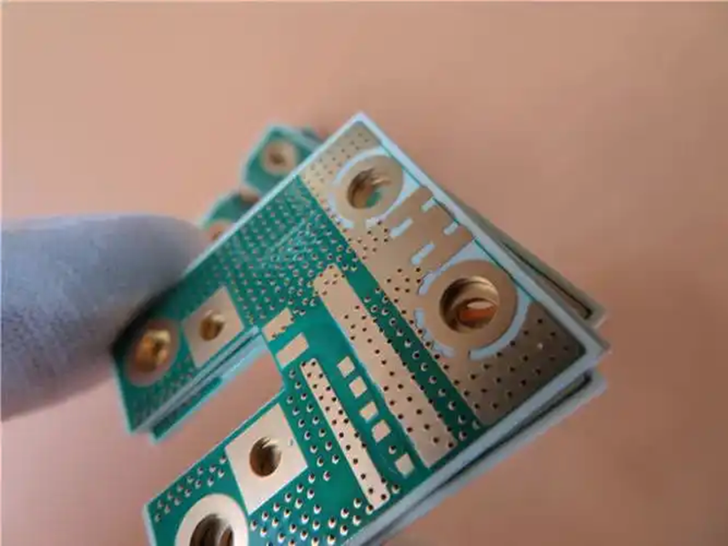
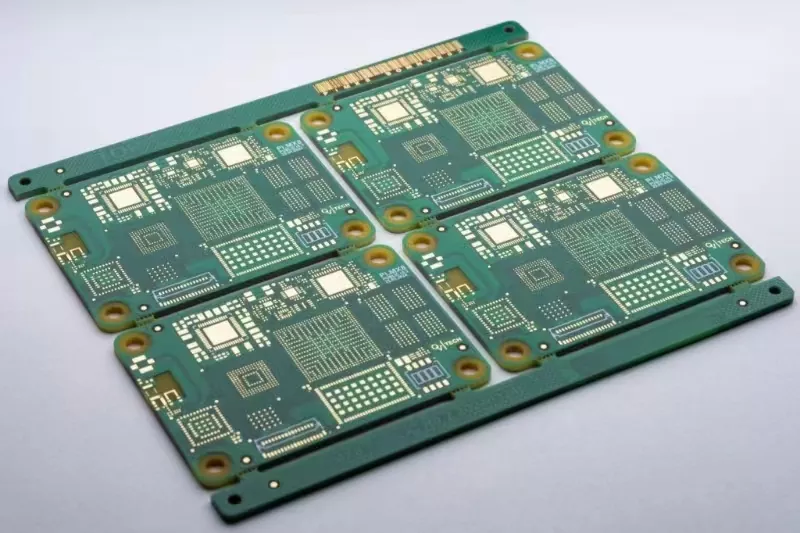
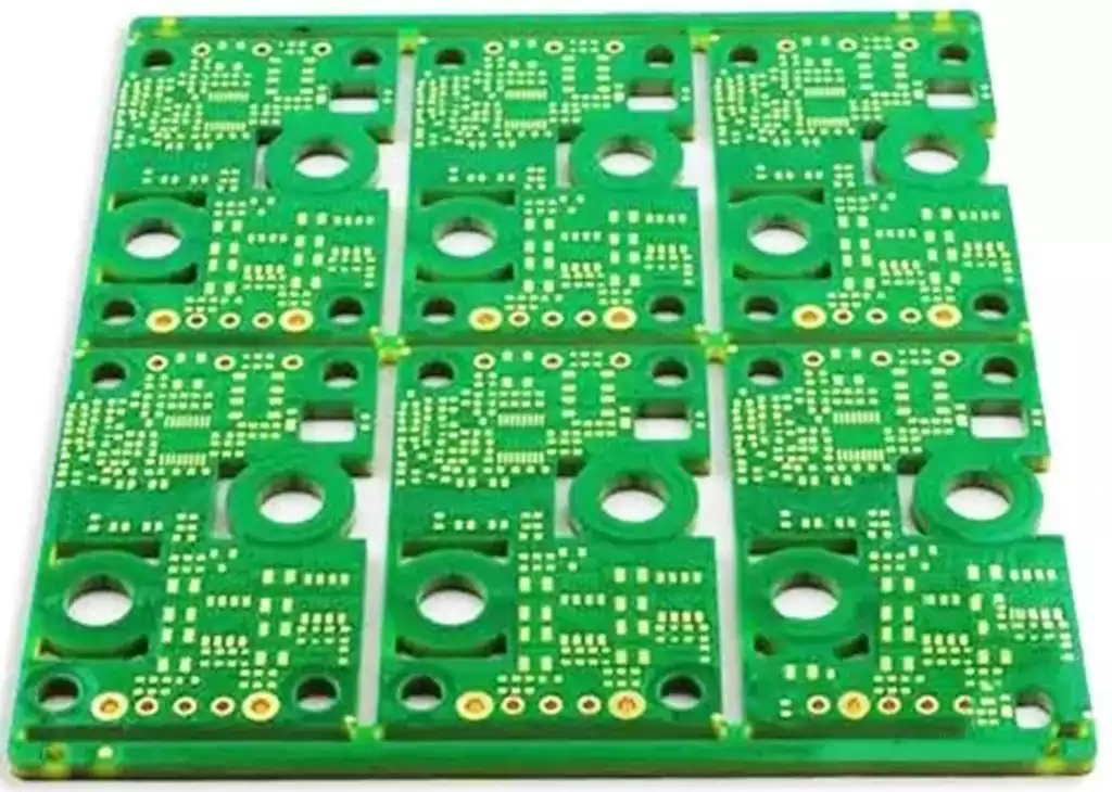
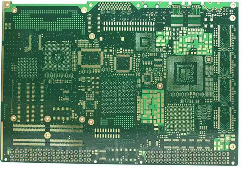
High multilayer circuit boards usually refer to circuit board structures with 10 to 20 or more layers. Compared with traditional multilayer circuit boards, the complexity of their processing processes has increased significantly, and the requirements for quality stability and long-term reliability are also more stringent. With excellent electrical performance and structural stability, these circuit boards are widely used in communications equipment, high-end servers, medical electronics, aerospace, industrial control and military equipment, and other key areas with stringent requirements for technical accuracy and system stability.
In recent years, under the continuous promotion of 5G communication network upgrading, speeding up the construction of base stations, intelligent aviation equipment, and modernisation of national defence and military industry, the market demand for high-level circuit boards has always maintained a strong growth trend. Along with China’s telecommunications equipment industry, technology iteration and market scale expansion, high-level circuit boards in the direction of high-frequency high-speed signal transmission, miniaturisation and integration, extreme environmental adaptability and other technological breakthroughs, is opening up a broader application space, the market outlook for the development of the industry is generally favourable.
High multilayer circuit board manufacturing process difficulties
Design complexity
Multilayer PCB design usually involves multiple circuit layers and complex signal paths, which makes the design process more complex. The design needs to consider the signal integrity of the interlayer, power distribution and thermal management issues, any design error may lead to board performance degradation.
Interlayer Alignment Difficulties
Inter-layer alignment difficulties due to the number of layers of high-level boards, the customer design side of the PCB layers of the alignment requirements are increasingly stringent, usually inter-layer alignment tolerance control ± 75μm, taking into account the design of high-level board unit size is larger, the graphic transfer workshop environment temperature and humidity, as well as the inconsistency of the different core board layer expansion and contraction of the misalignment brought about by the superposition of the inter-layer positioning methods and other factors that make the high-level board of the inter-layer alignment control is even more difficult.
Internal Circuit Manufacturing Challenges
- High-performance material requirements
Multilayer circuit boards often use high TG, high-speed, high-frequency, thick copper, thin dielectric layer and other materials, these materials on the internal circuit production and graphic size control put forward high requirements. For example, the integrity of impedance signal transmission requires precise control of line width and spacing to ensure signal transmission stability and efficiency. However, during rapid prototyping, it is often difficult to achieve the desired control accuracy due to time constraints. - Fine line signal layer and inner layer AOI inspection
Multilayer PCB circuit boards in the fine line signal layer, the AOI (Automatic Optical Inspection) requirements are extremely high. However, in the rapid prototyping process, due to time constraints, the inner AOI leakage detection probability increases, which may lead to some subtle defects are missed. In addition, the thin and wrinkle-prone inner core board, poor exposure and curling during etching also increase the difficulty of internal circuit manufacturing.
Thermal Management Issues
As the power density of electronic devices increases, thermal management issues become more prominent. Multilayer PCB in the working process may generate a lot of heat, how to effectively dissipate heat is an important factor that must be considered in the design and processing.
Drilling production accuracy specification requirements
- Drilling accuracy and surface roughness control
In the production of multilayer circuit boards, the drilling accuracy has extremely strict standards. Due to the increasing number of PCB layers, the total thickness of the copper layer is gradually superimposed, and during the drilling operation, the tool is very prone to breakage and the drilling edge is prone to burr. At the same time, the surface roughness of the drilled holes is also a key indicator of the quality of the PCB board. In the rapid prototyping stage, due to the tight schedule, it is often difficult to achieve accurate control of the drilling accuracy and surface roughness, and it is difficult to achieve the desired processing results.
2.CAF Failure and Drilling Tilt Problems
For PCB boards with dense BGA layout and narrow hole-wall spacing, CAF (conductive anode filament) failure is very easy to cause in the drilling process. In addition, as the thickness of PCB boards increases and the drilling accuracy is improved, the problem of tilted holes also occurs frequently. These problems not only adversely affect the quality of the PCB board, but may even lead to functional failure of the entire product.
As an important part of critical electronic equipment, its design and manufacturing process faces many technical challenges. Complex circuit design, strict layer alignment requirements, reliance on high-performance materials, and stringent drilling accuracy standards all impose high technical and quality control requirements on manufacturers. At the same time, with the continuous improvement of high-frequency, high-speed transmission and thermal management performance in the application field, the relevant processes and testing technologies need to be continuously optimised to safeguard the overall performance and reliability of circuit boards.
With the growth of demand in the fields of 5G, aerospace and defence, the market potential of high multilayer circuit boards is still significant, but its development must be based on technological breakthroughs and the maturity of the manufacturing process. Precise control of each production link and reasonable response to process difficulties are the key to ensure product quality and meet customer demand. The industry’s continued investment in technological innovation and quality improvement will be an important impetus to promote the steady development of high multilayer circuit boards.