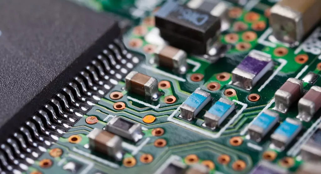
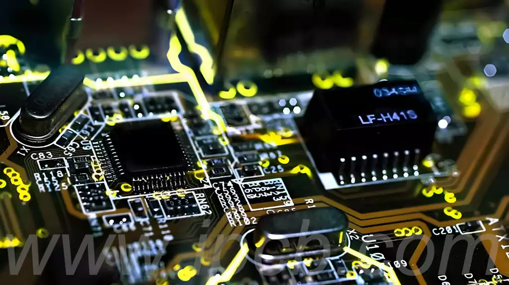
High voltage pcb design has an important position in modern electronic equipment, especially in the fields of power electronics, industrial control and new energy vehicles. As it involves high voltage and current, the design must strictly control key parameters such as creepage distance and electrical clearance to ensure the safety and long-term stable operation of the circuit. Reasonable selection of substrate materials, optimal layout design and the use of advanced manufacturing processes are key to ensuring the performance and reliability of high voltage PCB.
Creepage distance and clearance
Creepage distance and electrical clearance are important safety parameters in high voltage PCB design. Creepage distance refers to the shortest path length between the two conductive components along the insulating surface, while the gap is a straight line distance between the two through the air. Reasonable control of these two distances, effectively prevent the generation of arcs, to ensure the safe operation of the circuit. The design needs to take into account the operating voltage, environmental pollution level (such as dust, humidity) and material properties, usually refer to IPC-2221 and IEC-60950-1 and other international standards.
Choosing the right high voltage pcb material
Commonly used substrate materials in high voltage PCB design include BT epoxy, phenolic cured rigid laminates and high voltage polytetrafluoroethylene (HVPF). If other materials are being considered, special attention needs to be paid to their specification parameters, particularly the Relative Leakage Starting Trace Index (CTI), which is a key measure of the ability of an insulating material, such as a PCB substrate, to withstand dielectric breakdown near the surface. This index reflects the fact that the material begins to carbonise and become electrically conductive upon breakdown, leading to an increase in leakage current and accelerating the material’s damage process. International standards such as IEC-60950-1 and IPC-2221 recommend selecting suitable high voltage PCB materials based on the CTI value, which is typically measured by standard tests such as UL 746A, IEC 60112, or ASTM D3638, and its performance is divided into six class categories (PLCs) in order to provide guidance for design.
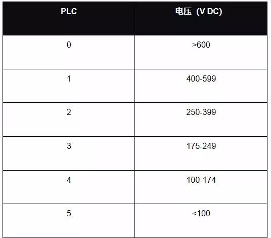
In fact, CTI provides you with a means of estimating the leakage current between two conductors when the conductor spacing is extremely small. It is important to note that the material degradation reflected in CTI is not the same as the dielectric breakdowns that initiate ionisation and subsequent current surges. These dielectric breakdowns occur at voltage levels much higher than those referred to by CTI, typically in the kilovolt range. Designs to withstand such high voltages should be made of at least PLC 0 rated materials to ensure long term reliability.
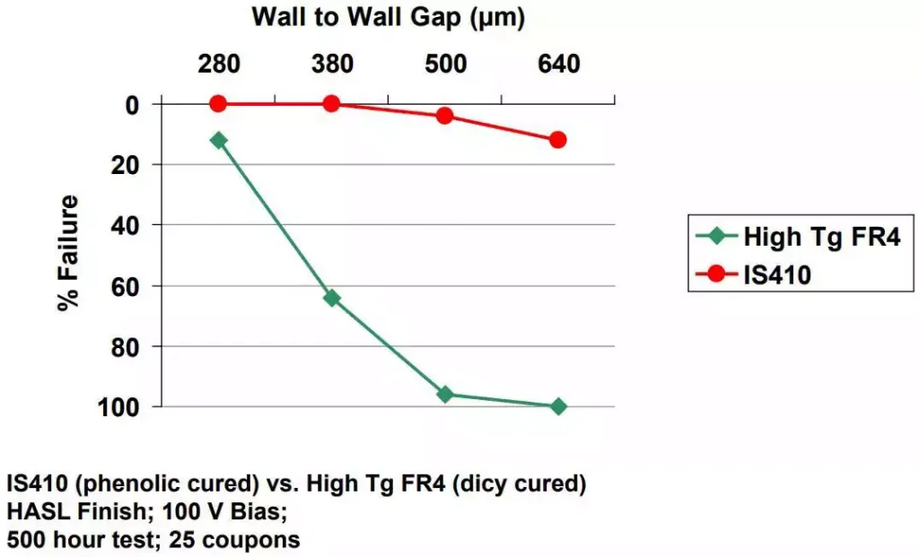
The material system consisting of resin content, glass weave and curing agent can significantly affect the reliability of a high voltage PCB design, especially the choice of resin content and curing agent. While FR4 laminates have been used in some high voltage PCB designs due to their higher breakdown voltage, they have lower CTI values (around 200-300 V DC) and are therefore considered a lower-end material option. Over time, the elastic properties of high-voltage PCB materials have become closely related to resin content and hardener, which is particularly critical in design for two reasons: firstly, high voltages promote metal migration and the formation of dendritic structures between conductors, leading to conductive anodic filamentation (CAF) failures; and secondly, lower resin content creates voids and increases the risk of degradation between layers of the PCB stack. High-voltage designs often tend to use substrates with higher resin content, resulting in a looser glass fibre weave. Glass transition temperatures (Tg) of up to ~180°C can be achieved in FR4 laminates cured with dicyandiamide (DICY), but these resin systems may fail earlier at high voltage gradients. Although some materials may have similar CTI values, laminates with phenolic curing agents exhibit lower failure rates and longer service life due to their ability to inhibit CAF growth.
Glass braiding is another key factor in the reliability of high voltage pcb. Finer glass braids, such as 1080, 2113 or 2116, are often ideal, while loose 106 braids may shorten the long-term life of the board. These glass braids ensure that the resin can flow and penetrate efficiently, while balancing the need to counteract conductive anodisation (CAF) at lower voltages.
With regard to surface finish and copper weight, copper must be of a quality that meets the requirements of high-voltage operation, and this includes both the choice of copper weight and the type of surface finish. Whether bare copper (generally not recommended) or a standard ENIG-like finish, the surface of the finished product should be as smooth as possible. This is because rough surfaces tend to accumulate static charge, which is not usually a problem for arcing or dielectric breakdown in low voltage environments, but can be a risk in high voltage situations. Manufacturers should provide expert guidance on plating materials and copper thickness for finished boards.
Copper weight is more important in applications involving high currents, although high voltages and high currents do not always occur at the same time. As the current intensity increases, the copper weight should increase accordingly. When currents in large circuit boards exceed approximately 100 A, bus bars are often required in place of conventional copper wiring. Using the IPC-2152 standard line diagrams is a good starting point for sizing PCB conductors, but be aware that the values recommended in the standard may be conservative and may not be applicable to all PCB designs!
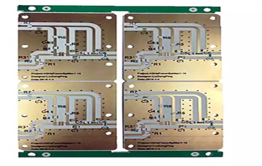
High voltage PCB layouts should be carefully designed to avoid sharp edges and irregular pad shapes in order to reduce the concentration of electric fields and thus reduce the risk of breakdown. In multi-layer designs, reasonable electrical gaps and creepage distances need to be maintained between internal layers, and uniform filling of the prepreg layer and the absence of air bubbles are key to ensuring insulation integrity. In addition, for high-current applications, appropriately thickened copper layers should be selected to meet current-carrying requirements, and combined with thermal management design to prevent overheating.
High voltage PCB design is a comprehensive engineering challenge, covering material selection, structural layout, electrical safety and thermal management. By scientifically and reasonably designing creepage distances and electrical gaps, selecting high-performance substrate materials, and combining thickened copper layers and good surface treatment technology, the safety and durability of the circuit board can be effectively improved. With the continuous progress of technology and application needs, high voltage PCB in various industries will be more widely used, its design and manufacturing level will continue to move towards higher standards.