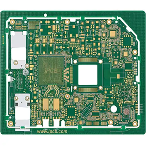
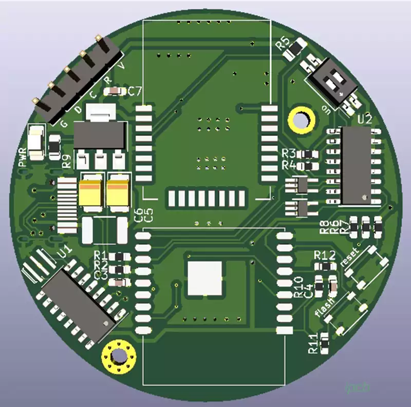
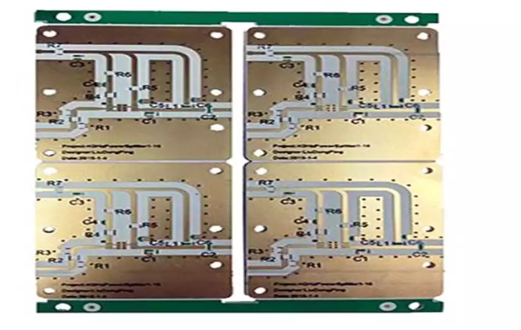
Printed Circuit Board (PCB) is an indispensable component of electronic equipment, which is made of insulating material in accordance with a predetermined design of conductive graphics, including printed circuit, printed components or a combination of both. This insulating substrate to provide electrical connections between the components of the conductive pattern, that is, known as the printed line. And the final finished board, we call the printed circuit board, referred to as printed circuit board or PCB. so, how do printed circuit board work?
Printed circuit boards work by combining electrically conductive and insulating materials to achieve the electrical connection of electronic components, so that electronic equipment can work properly. With the development of science and technology,circut board technology is also advancing, providing a strong support for the innovation of modern electronic equipment.
How are printed circuit boards made? All we need to do is open the keyboard of an ordinary computer to see a soft film (flexible insulating substrate) with a silver-white conductive graphic (silver paste) and key graphic printed on it. This graphic is obtained by the universal screen leakage printing method, so this printed circuit board is called flexible silver paste circut board.
However, the printed circuit boards we see in the computer market on various computer motherboards, graphics cards, network cards, modems, sound cards and household appliances are different. The substrates they use are mainly made of paper-based (commonly used for single-sided) or glass cloth-based (commonly used for double-sided and multi-layer) pre-impregnated with phenolic or epoxy resins, and then glued on one or both sides of the copper-clad foils, cured by lamination. This copper-clad sheet is called a rigid board, and the further processed printed circuit board is called a rigid printed circuit board. According to the distribution of printed circuit patterns, we can classify them into single-sided printed circuit boards, double-sided boards, and multilayer printed circuit boards. Multilayer boards are made of multiple layers of single- or double-sided printed circuit boards, alternately laminated with the help of positioning systems and insulating bonding materials, and interconnected with conductive graphics according to design requirements. Currently, there are more than 100 layers of practical printed circuit boards on the market.
The production process of printed circuit boards is quite complex, involving a variety of mechanical processing from simple to complex, chemical reactions and photochemical, electrochemical, thermochemical and other processes, while also requiring computer-aided design (CAM) and other aspects of knowledge. As the production process will continue to encounter new problems, and some of the problems in the cause has not been identified before the disappearance, coupled with its production process is a non-continuous assembly line form, any one of the errors may lead to a full line of production or a large number of scrap. The end-of-life printed circuit boards can not be recycled, which brings great pressure to the process engineers, resulting in many engineers choose to leave the industry, to the printed circuit board equipment or materials sales and technical service aspects of the work.
In order to better understand the PCB, we need to understand the single-sided, double-sided printed circuit boards and ordinary multilayer board production process
Single sided rigid printed circuit boards production process includes:preparation of single-sided copper-clad plate, material, brushing and drying, and then drilling or punching,followed by screen printing line resist etching graphics or the use of dry film and curing, followed by checking and repairing the board, etching copper after the removal of the resist printing material and drying, and then brushing and drying, followed by screen printing solder resist graphics (commonly used green oil) and UV curing, and then screen printing character marking graphics and UV curing, preheating Then screen print the character marking graphics and UV curing, preheating, punching and processing the shape, electrical open and short circuit test, brushing, drying, pre-coating flux anti-oxidant (drying) or spraying tin hot air levelling, and finally inspecting the packaging and leaving the factory.
Double sided rigid printed circuit board production process is more complex, including: preparation of double-sided copper-clad boards, undercutting, stacking boards, and then CNC drilling of pilot holes, inspection, deburring and brushing, followed by chemical plating (pilot hole metallisation) and full-board plating of thin copper, followed by inspection and brushing,screen printing of the negative circuit graphics and curing (dry or wet film, exposure, development), inspection and repair of the board after the line graphic plating and tin plating (corrosion-resistant nickel/gold), final inspection and packaging and shipment. Resist nickel / gold), remove the printing material (photographic film) after the etching of copper (tin), cleaning and brushing screen printing solder resist graphics (commonly used heat-curing green oil or paste photographic dry film or wet film,exposure,development,heat curing), cleaning and drying screen printing marking character graphics and curing, and then sprayed with tin or organic soldering film processing, processing and shape after cleaning and drying again, electrical on-off detection, and finally inspection and packaging and factory.
The multilayer board manufacturing process is based on the development of double-sided hole metallisation process,in addition to the inheritance of double-sided process,but also includes metallised holes in the inner layer of interconnections,drilling and de-epoxy drilling stains,positioning systems,laminating,and special materials and other unique content.
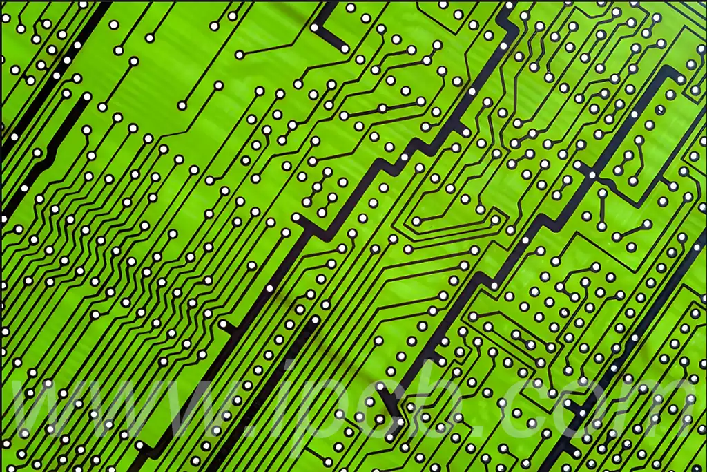
Our common computer boards are basically double sided printed circuit boards with an epoxy glass cloth base, where one side is used for inserting components and the other side is used for soldering component feet. These solder joints are very regular and the component foot soldering surface to which they correspond is called a pad.Why aren’t other copper wire graphics tinned? This is because,except for parts such as the pads that need to be soldered, the rest of the surface is covered with a solder resist film that is resistant to wave soldering. Most of this layer of solder resist film for the green,there are a few using yellow, black, blue and other colours,so in the PCB industry often solder resist oil called green oil. Its main role is to prevent wave soldering when the phenomenon of bridging, improve the quality of welding and save solder.At the same time,it is also a permanent protective layer of the printed circuit board, can play a role in moisture, corrosion,mildew and prevent mechanical abrasion.From the appearance,the surface of the smooth and bright green solder resist film is usually made of film on the board sensitised thermal curing green oil.This green oil is not only beautiful in appearance,but more importantly,its pad accuracy is higher, thus improving the reliability of the solder joints.
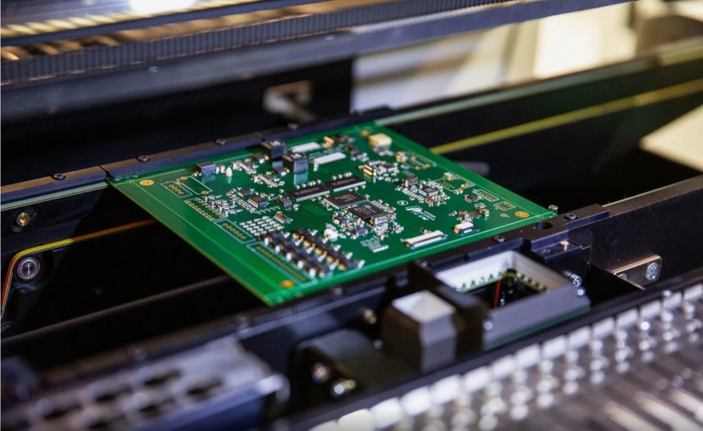
From the computer board we can see that the installation of components there are three main ways: the traditional insertion of the installation process, the surface mounting process and chip direct mounting technology.Among them, the chip direct mounting technology can be regarded as a branch of the surface mounting technology, it is the chip directly pasted on the printed board, and then through the line welding method, carrier tape method, flip-flop method, beam lead method and other packaging technology interconnected to the printed board. Its welding surface is on the component surface.
Printed circuit boards as a key component of electronic equipment, its exquisite working principle and complex manufacturing process together to support the progress of modern technology. In the face of escalating market demand and technological challenges, the PCB industry is continuing to innovate and promote electronic equipment to a higher level of development.
