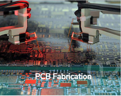
Introduction
The circuit board, or printed circuit board (PCB), is the backbone of modern electronic devices. From smartphones to computers, PCBs are integral components that allow electronic devices to function. This guide will walk you through the detailed process of how a circuit board is made, covering every step from design to final assembly.
The process begins with designing the PCB layout. Engineers start with a schematic design, which is created using specialized software such as Altium Designer or Eagle. This diagram maps out the electrical connections between components. Once the schematic is completed, it is converted into a PCB layout. This step involves determining the physical placement of components and routing the electrical connections. Design rules are applied to ensure the board is manufacturable and reliable. The layout then undergoes a Design Rule Check (DRC) to identify and rectify any design issues, ensuring compliance with manufacturing standards.
Material Selection
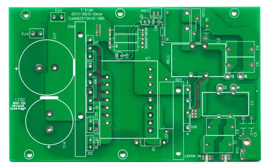
Choosing the right materials is crucial for the performance and durability of the PCB. The base of the PCB, typically made of fiberglass (FR4) or other insulating materials, provides mechanical support. A thin layer of copper is laminated onto the substrate to form the conductive pathways. Additional layers, such as a solder mask, protect the copper traces from oxidation and prevent short circuits. Printed text and symbols, known as the silkscreen, provide component labels and other essential information.
Printing the Design
The PCB design is transferred onto the copper-clad board using a process called photoresist. This involves applying a light-sensitive material, known as photoresist, to the copper surface. The board is then exposed to ultraviolet light through a photomask containing the PCB design. The light hardens the exposed photoresist. The board is subsequently developed, removing the unexposed photoresist and leaving the hardened resist to protect the desired copper areas.
Etching
Etching is the process of removing unwanted copper from the board, leaving only the copper traces that form the circuit. The board is submerged in an etching solution, such as ferric chloride, which dissolves the unprotected copper. After etching, the board is thoroughly cleaned to remove any remaining photoresist and etching solution residues.
Drilling
Precise holes are drilled into the PCB for component leads and vias (connections between layers). This step utilizes computer-controlled drilling machines to ensure accurate hole placement and size. Once drilled, the holes are plated with copper to establish electrical connectivity between layers.
Plating and Coating
Additional plating and coating steps are undertaken to enhance the board’s performance. A thin layer of additional copper is electroplated onto the traces and through-hole walls. Following this, the solder mask is applied to protect the copper traces and prevent solder bridges during component soldering. Various surface finishes, such as HASL (Hot Air Solder Leveling) or ENIG (Electroless Nickel Immersion Gold), are applied to the exposed copper pads to improve solderability and protect against oxidation.
Silkscreen Printing
The silkscreen layer is applied to add text and symbols to the PCB, providing information such as component identifiers, logos, and warnings. This involves using a stencil to apply the silkscreen ink to the board, which is then cured to harden the ink.
Testing
Before components are assembled, the bare PCB undergoes several tests to ensure it meets quality standards. Automated electrical tests check for shorts, opens, and correct resistance values in the copper traces. Additionally, optical inspection systems or manual checks identify any physical defects or misalignments.
Component Assembly
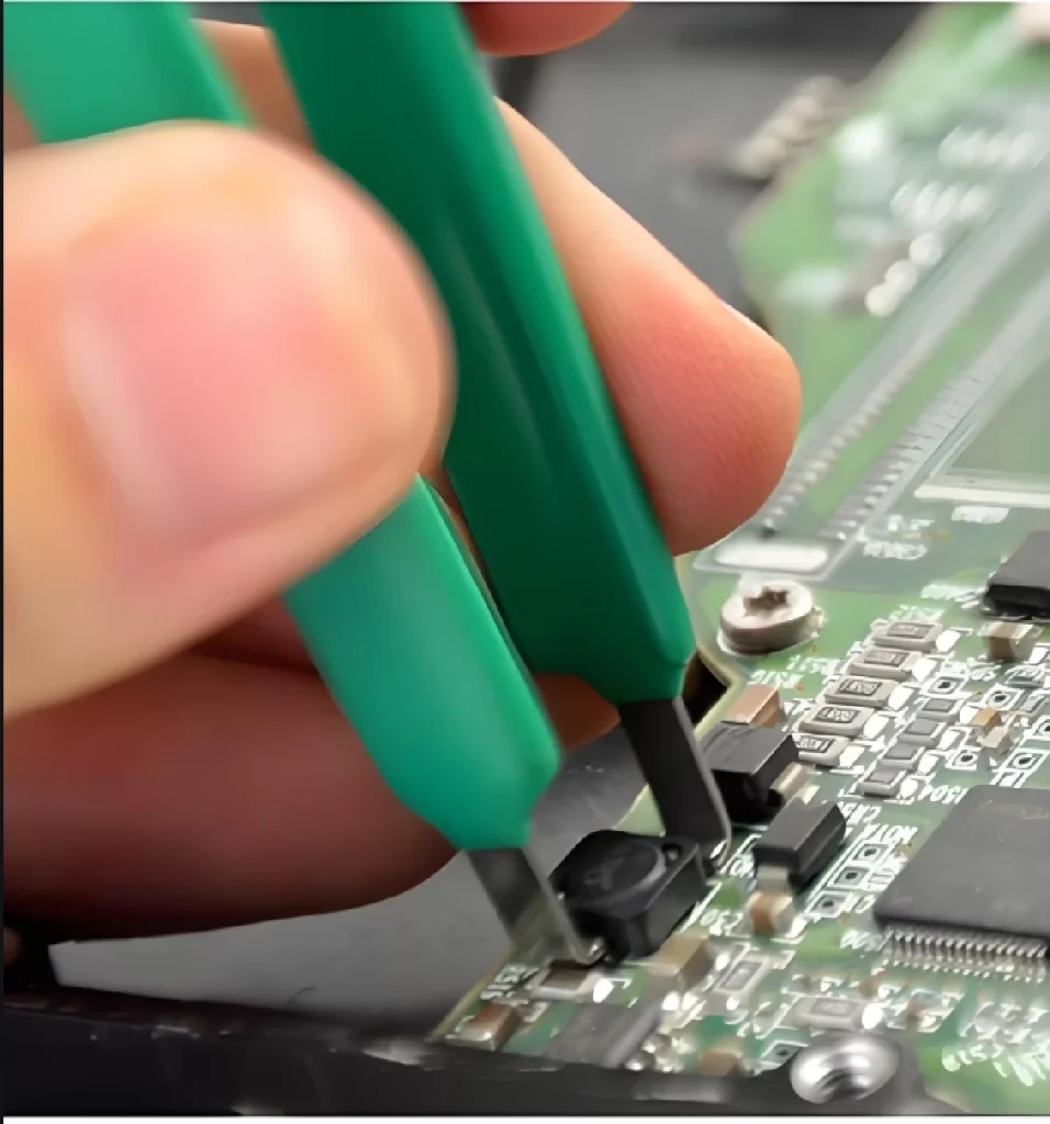
With a validated PCB, the next step is to assemble the electronic components. Solder paste is first applied to the pads using a stencil. Then, pick-and-place machines position components onto the board with high precision. The assembled board is then heated in a reflow oven, melting the solder paste and forming reliable solder joints. Automated optical inspection (AOI) and X-ray inspection systems verify the quality of solder joints and component placement.
Final Testing and Quality Assurance
The assembled PCB undergoes final testing to ensure it functions correctly. Functional testing involves testing the board in a simulated operating environment to verify its performance. Burn-in testing may also be conducted, where boards undergo extended operation under stress conditions to detect early failures.
Packaging and Shipping
After passing all tests, the PCBs are ready for packaging and shipping. The boards are cleaned to remove any flux residues or contaminants. Conformal coatings may be applied to protect the board from environmental factors. Finally, the PCBs are packaged to prevent damage during transportation and handling.
Conclusion
Manufacturing a circuit board is a complex, multi-step process that requires precision, expertise, and stringent quality control. From design and material selection to assembly and testing, each stage plays a crucial role in ensuring the final product meets the required standards and functions as intended. Understanding these steps not only highlights the intricacies involved in PCB manufacturing but also underscores the importance of quality at every stage to deliver reliable and high-performance electronic devices.