How is an integrated circuit made? Integrated circuits are based on a planar process and are formed through multi-layer processing. At present, the vast majority of integrated circuits are made on a single crystal silicon substrate, i.e., silicon-based integrated circuits, which are made from a single silicon wafer (chip or wafer) as a unit, a silicon wafer (wafer) contains a lot of integrated circuits chip (chip, die).
The main process of integrated circuit design and manufacturing
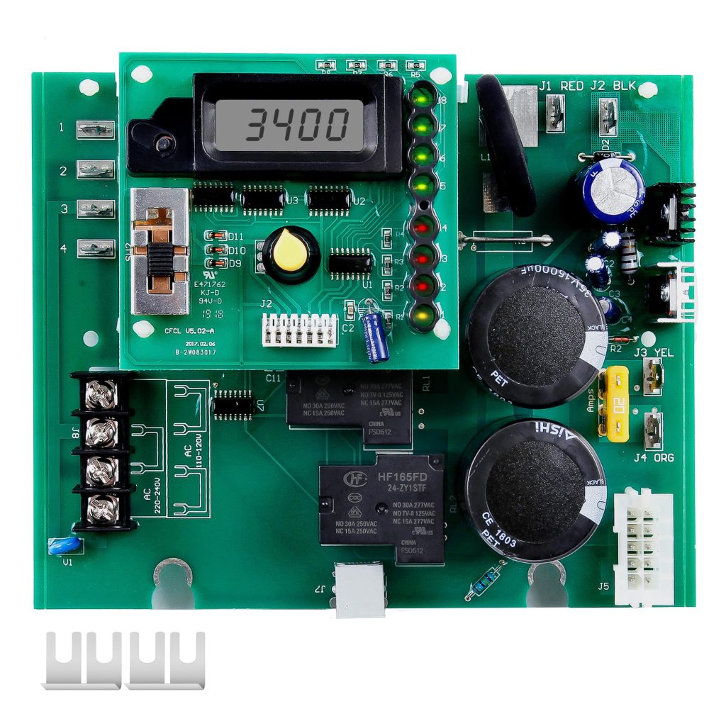
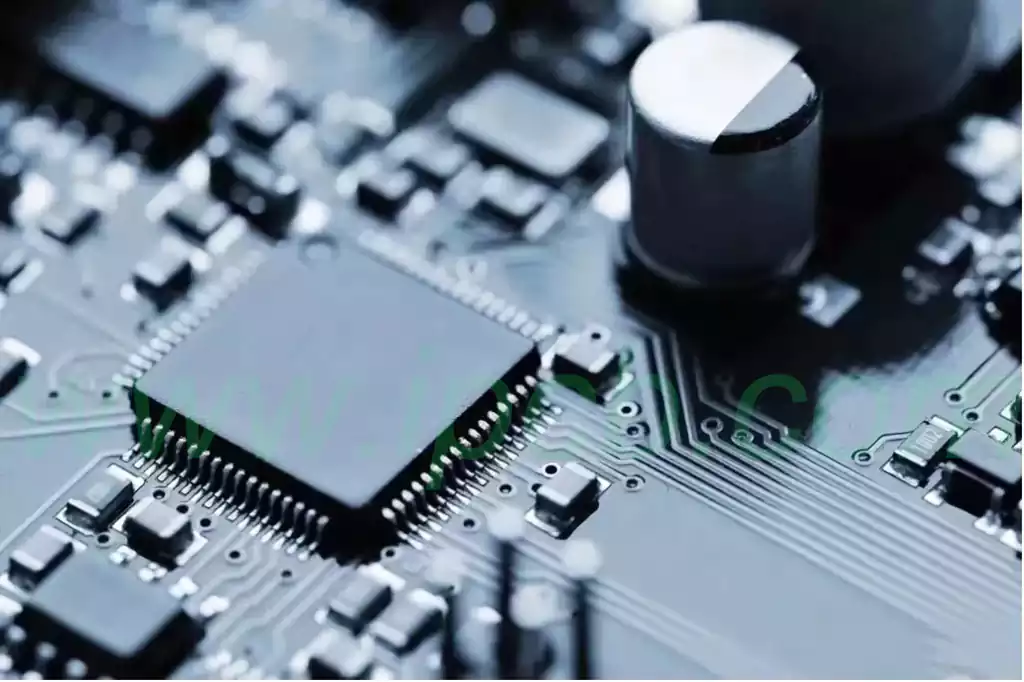
The birth of a chip can be divided into three links: chip design, chip manufacturing and packaging.
Chip Design
Customers put forward the design requirements, IC design engineers to complete the design of the logic circuit, the design will be converted into circuit diagrams, software testing and verification to see whether it meets the customer’s needs, and finally the circuit diagrams in the form of photomasks, for the next step in the manufacture of the use.Chip Manufacturing
IC manufacturing is divided into two major segments: wafer manufacturing and wafer processing.
Wafer (wafer), is the basis for manufacturing various types of computer chips.We can imagine chip manufacturing as building a house with Legos, i.e., by stacking one layer after another to complete the desired shape (i.e., various types of chips).In order to make a perfect,solid house,we need a good foundation, that is, a smooth substrate. For chip manufacturing, this substrate is the “wafer”.
Wafer manufacturing is the process of making monocrystalline silicon wafers using silicon dioxide as the raw material.Monocrystalline silicon wafer production process is: crystal pulling – roller grinding – wire cutting – chamfering – grinding – corrosion – heat treatment – edge polishing – front side polishing – cleaning – testing – epitaxial and other steps, of which crystal pulling, grinding and polishing is to ensure the quality of semiconductor wafers is the key.
Wafer Processing: refers to the process of making logic circuits on wafers. Diffusion, deposition, photolithography, etching, ion implantation, polishing, metallization and other operations are carried out on silicon wafers, all of which are carried out in wafer clean plants.
IC Sealing
The process of thinning,cutting,patching,lead bonding,encapsulation, and testing of wafers.The last process of semiconductor manufacturing is testing, and the testing process can be divided into preliminary testing and final testing,the main purpose of which is to ensure that customers want goods without shortcomings, but also according to the specifications of the classification of IC grade.The finished product of the final test will be labeled with the specification and packaged for delivery to the customer.Products that do not pass the test will be downgraded or discarded.
Factors to consider in IC design
- Meet the requirements of function and performance (performance: speed, power consumption)
- Reduce chip cost (including: design, manufacturing, testing)Design: a good design flow will reduce the design cost of the chip.
Manufacturing: need to optimize the design to reduce the chip area, increase the number of cores on each wafer, and use DFM methods in the design to improve the chip manufacturing yield.
Testing: Design for Testability (DFT) methodology is used in the design to reduce the testing time of each chip.
Calculation of single-chip cost: CT = CD/N + CP/(y*n) + package test cost
The first term represents the design cost allocated to each chip: CD is the design and mask plate cost (also called NRE cost), and N is the total production volume;
The second item indicates the manufacturing cost per chip: CP is the manufacturing cost per wafer, n is the number of cores on each wafer, and y is the wafer yield; - Extend the life of the chip
- Shorten the chip time to market (Time-to-Market)
The integrated circuit design flow is the process of translating the functional requirements of a circuit into a circuit design and ultimately a physical chip. The following is a typical IC design flow:
Requirements analysis: Determine the circuit’s functional requirements, performance specifications, power consumption requirements, etc.
Conceptual design: Based on the requirements analysis, conduct circuit architecture design to determine the basic functional modules of the circuit and the connection relationship.
Circuit design: detailed design of each functional module, including the selection of appropriate devices, design circuit topology and circuit parameters, circuit simulation and optimization.
Physical Design: Translate circuit design into physical layout, including the placement of circuit modules on the chip, designing circuit connections and vias, etc.
Circuit Verification: Verify that the function and performance of the circuit meets the design requirements through circuit simulation and actual testing.
Manufacturing Preparation: Generate mask graphics required for manufacturing, perform process rule checks and circuit layout rule checks, and prepare documents required for production.
Manufacturing production: According to the documents prepared for manufacturing, the chip is manufactured,including photolithography,thin film deposition, diffusion and other process steps.
Packaging test: Packaging the chip into the final package form, testing and quality control.
Finished product testing: Conduct final functional and performance tests on the packaged chip.
Product Release: Deliver the chip to the customer or market the product for sale.
How is an integrated circuit made
The processing of integrated circuits involves three basic operations.
Formation of a film of some material
In the integrated circuit production process to form a silicon dioxide film, polycrystalline silicon film, silicon nitride film, some metal silicide film and as a link to the metal film, and so on. The method of forming these films is mainly chemical vapor deposition (Chemical Vapor Deposition, abbreviated as CVD) or physical vapor deposition (Physical Vapor Deposition, abbreviated as PVD). However, the formation of high-quality films is achieved by thermal oxidation, in which silicon atoms react with oxygen at high temperatures to form silica, i.e.
Here the oxygen is fed into the reaction chamber from outside, and the silicon is the silicon atoms in the wafer, so the thermal growth to form SiO consumes the silicon in the substrate. The film formed by the precipitation method is uniformly covered over the entire wafer, whereas by the oxidation method the film can be formed only in localized areas.
Formation of desired patterns on various thin-film materials
The processing of graphics is accomplished by photolithography and etching processes. Lithography and etching is a very important process in the integrated circuit processing, integrated circuits can continue to comply with Moore’s law to move forward, largely determined by the photolithography and etching process can continue to achieve smaller line graphics.
The role of photolithography and etching is to copy the graphics from the designed IC layout onto a silicon wafer. Current lithography is primarily optical lithography, which transfers the graphics from the mask plate to the silicon wafer. The principles of photolithography and etching are illustrated below as an example of forming a pattern on an oxide layer. The wafer, which has grown a film, is used to form the desired pattern on the oxide layer in several basic steps:
Dumping – a uniform layer of photoresist is applied to the surface of the wafer.
Exposure – the coated wafer is placed under a mask plate and exposed to light (usually ultraviolet light), so that the photoresist corresponding to the bright (clear) areas on the mask plate is exposed, while the photoresist corresponding to the dark areas on the mask plate cannot be exposed. Therefore, the mask plate acts as a photographic backing plate. If a negative adhesive is used, the exposed photoresist undergoes a polymerization reaction that makes it stronger and less likely to be removed.
Developing – removing the unexposed adhesive (for negative adhesive) by chemical or physical means. After developing, the image on the mask is transferred to the photoresist.
Etching – removing the part of the mask that is not protected by the photoresist. After etching, the image on the mask is transferred to the film. In the past, chemical solutions were used for etching, hence the name wet etching. Wet etching can not accurately control the etching rate, it is difficult to achieve fine graphics. Currently, dry etching is used in integrated circuit processing, such as reaction ion (Reaction Ion Etching, referred to as RIE) etching.
Degumming — finally remove all the photoresist residue on the wafer, you get the completion of some kind of graphic processing of silicon wafers.
The photolithography described above is for the case of negative adhesive. Positive adhesives are usually used to realize high-resolution graphics. Positive adhesive has the opposite properties of negative adhesive, in that the photoresist that is exposed to light during exposure undergoes a decomposition reaction and is easily removed during development, while the photoresist that has not been exposed remains after development. Therefore, for the same mask plate, with negative and positive adhesive on the wafer to get the opposite pattern.
Changing the resistivity or impurity type of a material through doping
The resistivity of a material can be changed by diffusion or ion implantation in the fabrication of integrated circuits, or by changing the type of localized impurities to form pn junctions. In order to avoid the impact of high temperature processes on device and circuit performance, the current integrated circuits are mainly doped by ion implantation (doping). Ion implantation is carried out at room temperature, however, after ion implantation requires high-temperature annealing, rapid thermal annealing can be used to reduce the high-temperature processing time. Doping process is also very important for integrated circuits, because the conductivity of the semiconductor with the type of impurities and the number and distribution of impurities are closely related.
In short, integrated circuits are made by forming a film of a certain material, forming the desired pattern on the film, and doping the film or a localized area of the wafer in a number of basic processes.
How is an integrated circuit made, this complex and delicate process, not only reveals the mystery of modern technology, but also highlights the determination of mankind to constantly pursue excellence. From design to manufacture, every step of the way, cohesion of the wisdom of engineers and sweat, together cast this important cornerstone to promote social progress.