As a core component, the design and layout of an integrated circuit board (IC board) has a direct impact on the performance, reliability, and productivity of the device.The layout of IC board components not only needs to meet the requirements of electrical performance, but also needs to take into account various factors such as manufacturing process, heat dissipation management, and signal integrity. With the development of electronic devices in the direction of miniaturisation and high performance, the design of IC boards has become more and more complex, and how to optimise the component layout has become an important challenge for engineers.
Basic Principles of IC Board Component Layout
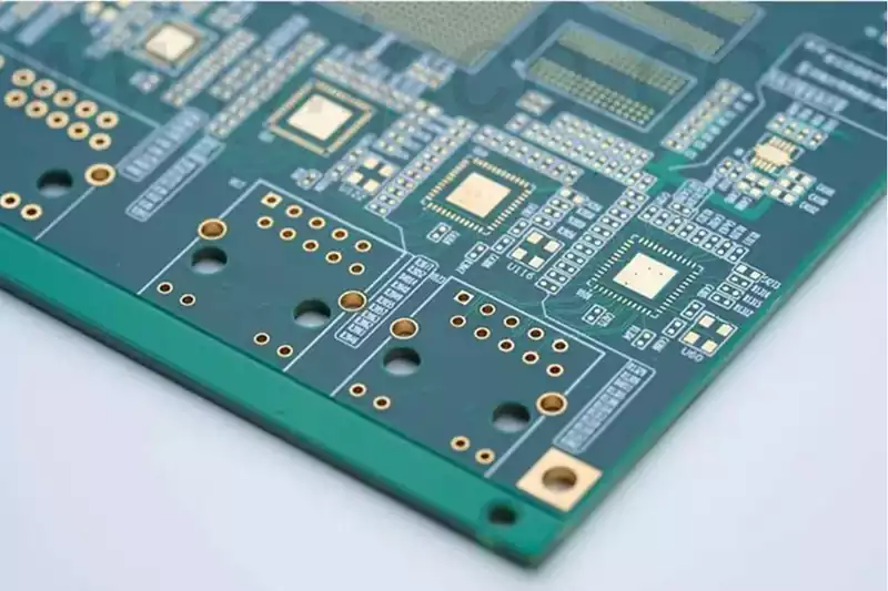
Component spacing: IC board components should be properly spaced, usually recommended between 0.35 inches to 0.5 inches, larger ICs need more space to avoid signal interference and heat dissipation problems.
Functional Partitioning: Components should be partitioned and laid out according to the functional modules of the circuit, such as separating the power module, signal processing module and communication module to reduce noise interference.
Signal integrity: High-speed signal lines should be as short and straight as possible to avoid crossing with other signal lines, while keeping sensitive components away from high-noise areas.
Method of placing IC board components:
- When designing the circuit board, the spacing between integrated circuits should be kept between 0.35 inches and 0.5 inches, and for larger integrated circuits, the spacing should be increased appropriately.
- In order to simplify the subsequent installation inspection and testing process, components with similar functions should be arranged in the same direction.
- During layout, components should be isolated according to the functional modules of the circuit to ensure that there is sufficient distance between high noise signals and highly sensitive signals.
- Priority should be given to the layout of edge components to facilitate input and output connections to the circuit board.
- Due to the different impedance characteristics of circuit board edges, sensitive high-speed devices should be avoided to be placed close to the edge to reduce electromagnetic interference (EMI), it is recommended that they be placed in the centre area of the board.
- In high-frequency circuit design, the connection line between the components should be as short as possible and close to the device, but need to pay attention to avoid local overheating problems caused by the line is too short, can be through the components and the parallel layout of the heat pipe to dissipate heat.
- Avoid overlapping components to prevent the risk of short-circuit caused by current flow.
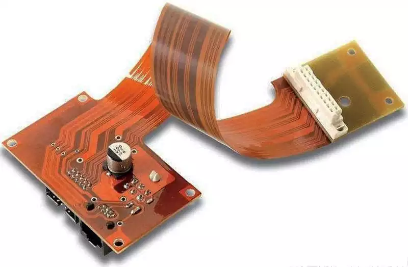
- Considering the weight and space constraints, multi-layer circuit boards are a common choice, but be aware that multi-layer layouts may increase costs due to soldering process limitations.
- When laying out components, enough space should be reserved for copper wires to pass through.
- According to the logic group on the circuit board layout components, similar to the schematic design, can effectively save time and reduce the length of the line.
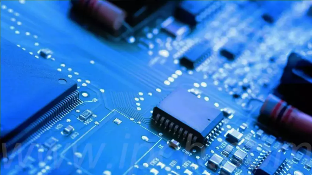
The chip assembly process is a critical part of electronics production.IC board component assembly is the process of mounting the chip on the circuit board, including placement, soldering and testing steps. Specific process of chip assembly.
SMD process: first of all, the use of automatic mounter will be the original chip from the feeder, and according to the circuit board design drawings and pad location, accurate chip mounting to the circuit board in the specified location. This process requires a high degree of precision in the equipment to ensure that each chip is placed accurately.
Soldering process: After the chip is placed, the chip needs to be soldered to the circuit board. Common soldering methods include Surface Mount Technology (SMT) and Through Hole Technology (THT); SMT connects the chip pins to the pads by melting the solder paste, which is suitable for small chips and high-density circuit boards; THT inserts the chip pins into the through holes of the circuit boards for soldering, which is more suitable for larger chip sizes.
Testing: After the chip is assembled, functional and reliability tests are required to verify its performance and quality. Functional tests cover electrical characteristics, signal integrity and performance indicators to ensure that the chip functions properly. The reliability test assesses the stability and service life of the chip in actual applications by simulating different environmental conditions.
The layout and design of IC board components is a key aspect in the development of electronic devices, and its optimisation not only enhances circuit performance, but also reduces production costs and improves product reliability. By following design principles, solving common problems, and combining advanced manufacturing processes, engineers can design high-performance, high-reliability IC boards.