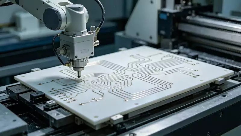
The tin spraying process, also known as hasl, is a long-established technology for PCB (Printed Circuit Board) surface treatment. The process starts by immersing the PCB in molten solder, which is then applied to the copper surface, followed by the use of a hot air gun to blow away the excess solder material, resulting in a uniformly distributed film of solder on the surface of the PCB.
HASL Process
Prior to the HASL (Hot Air Surface Levelling) surface treatment, the first step is to thoroughly clean the PCB, which is usually achieved by micro-etching techniques to remove impurities from the copper surface. Once the cleaning is complete, the PCB goes through a preheating phase and is coated with a layer of flux. The purpose of the flux is to reduce the surface tension between the PCB board and the solder, thus enabling the solder to adhere more evenly to the PCB.
Immediately thereafter, the flux-coated PCB is immersed in a molten tin/lead alloy solution, at which point the exposed copper pad area is covered by the tin/lead solution, forming a tin-lead alloy layer. After completing the tin dipping step, using the high pressure hot air knife of the hot air levelling machine, excess solder on the surface of the PCB board and in the holes can be removed to ensure the uniformity of solder deposition, ultimately leaving a layer of protection on the pads that is both uniform and thin.
Key parameters of the HASL process include:
Solder temperature: the melting point of the Sn63Pb37 alloy is 183°C. To ensure the formation of good intermetallic compounds, the solder temperature is usually set in the 230-250°C range.
Soak time: This process is generally controlled between 2-4 seconds to avoid overgrowth of intermetallic compounds.
Hot Air Knife Pressure and Flow Rate: The higher the pressure and flow rate of the hot air knife, the thinner the thickness of the solder coating, usually the pressure of the hot air knife is controlled between 0.3-0.5MPa.
Hot Air Knife Angle: the choice of angle is critical, improper angle will lead to uneven coating thickness on both sides of the PCB board, generally the hot air knife will be adjusted downward by 4° to optimise the coating effect.
Hot Air Knife Pitch: This pitch is usually set at 0.95-1.25cm.
PCB rising speed: This speed should be adjusted flexibly according to the actual situation. A slower rise speed will increase the hot air processing time, resulting in a thinner solder layer; conversely, it may result in a thicker solder layer.
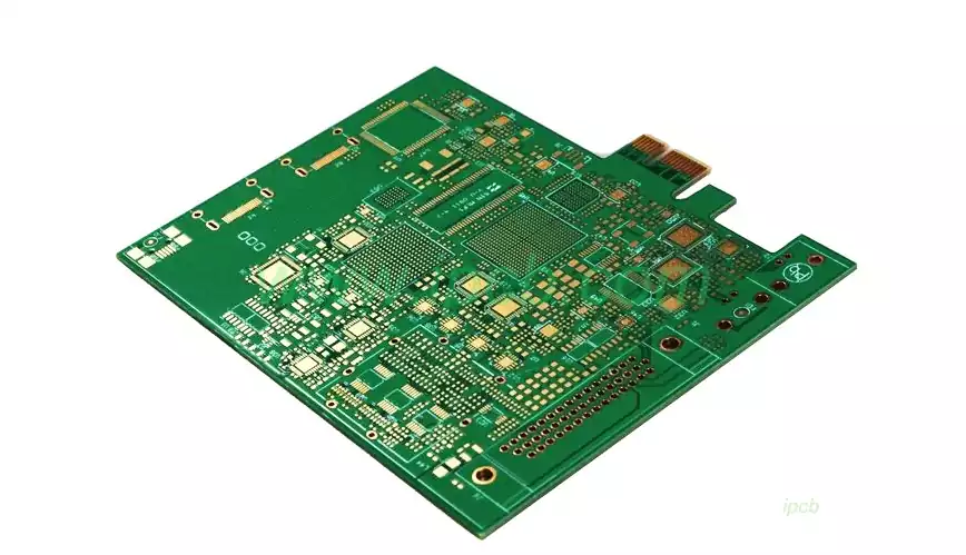
The impact of hasl process on PCB board
- Solderability Enhancement
A central tenet of the tin spray process is to enhance the solderability of PCB pads. The process involves spreading molten tin-lead alloy (or lead-free tin alloy) uniformly over the surface of the PCB copper foil in a spraying manner, thus forming a layer of bright tin plating. When soldering electronic components, this layer of tin can quickly fuse with the solder material to create a solid connection between the electronic components and the PCB. To consumer electronics in the field of mobile phone motherboard manufacturing, for example, a large number of tiny chip components need to be accurately welded in place, and after the hasl treatment of the pad to ensure that the solder paste in the reflow soldering process to achieve a good wetting effect, significantly reduce the incidence of welding defects such as false soldering, bad soldering, to a large extent to improve the production efficiency and product qualification rate for the construction of complex circuitry system provides a reliable guarantee. - Anti-oxidation and corrosion resistance
Tin material itself has certain antioxidant properties, hasl process for the PCB surface to add a layer of ‘protective cover’, effectively blocking the external environment of oxygen, moisture and other corrosive factors. For those long-term operation in harsh working conditions of industrial control PCB, such as factory automation equipment control boards, outdoor power monitoring equipment, circuit boards, etc., tin spray layer can be maintained for a long time pads and lines of the metal luster, to prevent the copper foil suffered oxidation rust trouble, to avoid corrosion triggered by the line circuit breakers or poor contact and other faults, and thus ensure that the equipment at high temperatures, high humidity, dust and other complex environments, stable operation, extending the PCB. This ensures the stable operation of the equipment in high temperature, high humidity, dusty environment and prolongs the service life of PCB. - Electrical Characteristics Improvement
From the dimension of electrical characteristics, hasl process shows the same significant advantages. Uniformly coated tin layer with excellent conductivity, compared with the bare copper foil, can more effectively reduce the contact resistance of the line, to ensure the smooth flow of current in the PCB. Especially in high-frequency circuits, although the tin layer does not have the extremely low loss characteristics of some specialised high-frequency materials, it is able to compensate for small defects on the surface of the copper foil, making the current path smoother, thus inhibiting signal reflection and scattering to a certain extent, and helping to maintain the integrity of the signal. This plays an active role in improving the performance of high-end products such as RF front-end PCBs for 5G communication base stations and high-speed computer motherboards. - Mechanical Protection Efficiency
In the subsequent process of PCB, assembly process and the actual application of the period, it will inevitably encounter a variety of mechanical impact, such as the insertion and removal of components, vibration interference in transit, etc.. Tin spray layer in this process plays a key role in the buffer and protection, it is like for the PCB cloak a ‘protective cover’, effectively mitigating the direct impact of external forces on the copper foil and its lines, significantly reducing the line fracture, solder pad peeling risk. Server motherboards, for example, in view of its hardware upgrades and maintenance of frequent, which means that the interface parts will experience a lot of insertion and removal operations, hasl process in this case for the pad to provide strong protection to ensure that the server after a long period of time, high-intensity use, but still be able to maintain a reliable operating state. - Surface flatness limitations
Compared with some advanced surface treatment technology, hasl process in the surface flatness of certain deficiencies, may not be able to meet the needs of high-density, fine-pitch circuit design. When soldering precision electronic components, the unevenness of the surface may affect the quality and reliability of the soldering, thus becoming a factor restricting its application.
The hasl process plays multiple key roles in PCB manufacturing, but also faces the challenge of surface flatness. As technology evolves, PCB manufacturers need to continue to optimise the tin spray process and explore new technologies to meet the growing market demand for high performance PCB boards.