In modern electronic devices, power management boards are key to maintaining stable operation. As the functions of devices become more and more abundant, a single power input must support multiple output modules, which puts higher requirements on the flexibility and reliability of the distribution structure. In this context, the PCB splitter, a distribution structure based on line design, is particularly important
What is a PCB splitter? In a power supply board (Power Supply PCB), it is a design method that efficiently and safely distributes an input power (or signal) to multiple sub-modules through lines, jacks, slots or other conductor structures. It is different from an active electronic distributor and does not require chip control; instead, it uses PCB paths to achieve “high-fidelity distribution” of current/signals. Especially when the design contains multiple power paths, PCB splitters can significantly improve electrical performance, save space, and improve overall reliability.
For a simple example: on a 12V power board, if you want to power the main controller, relay module, USB charging module and sensor, through the PCB splitter design, you can achieve multi-point branching on the same board to avoid single-line carrying too much current or bulky and messy cables.
This article will start from six major systems, including structural principles, design process, manufacturing process, performance analysis, test verification and optimization direction, to help technicians, purchasing engineers and newcomers in the industry to deeply understand the core value of PCB splitters in power board positions and master practical design experience.
PCB splitter structure and principle
Basic structure of splitter
PCB splitters have many implementation methods, including:
Line type split structure: multiple branches are formed by wide copper wire branches, each branch is designed with appropriate line width and impedance control, used for large current distribution;
Jack split structure: slots or grooves are dug on the PCB to isolate different areas or make switch/connector connections, suitable for power distribution of sensors or modules;
Double-sided/multi-layer split structure: using a multi-layer PCB structure, the input is introduced from the top layer, multiple output paths are separated in the inner layer, and then returned to the top layer or lower layer;
Removable bridge structure: designed as a bridge that can be welded or plugged in, supporting function customization, iterative fast switching and flexible debugging.
Electrical principle
PCB splitter design needs to ensure that each path can stably transmit the required voltage and current without significant voltage drop. For example, a 12V/5A input line is divided into three branches, providing 2A, 1A, and 2A to different modules respectively. During design, a comprehensive evaluation of line impedance, current density, and heat load is required to ensure that it will not cause overheating, excessive pressure loss, or exceed the board’s carrying capacity.
Important design indicators
When designing PCB splitters, the following key indicators are often concerned:
Line width and current carrying capacity: Refer to the IPC-2152 standard to determine the copper thickness and line width required for each branch;
Resistance and voltage drop: Increased resistance will cause the input voltage to drop, affecting module performance;
Thermal management capability: Especially for large current branches, it is necessary to consider copper wire heat dissipation and board area occupation;
Isolation and anti-interference: For high-frequency or high-noise modules, isolation walls or slotted structures need to be designed with power distribution;
Testability and debugging convenience: In some scenarios, it is necessary to add test points, jumper holes and other modules to each branch.
Manufacturing process and design rules
Board selection and copper thickness configuration
PCB shunts are often used in power circuits, so the board needs to have high current carrying capacity and thermal stability. Common material choices include:
FR-4 standard board: suitable for general electronic equipment and medium and low power circuits.
High Tg board (such as TG170, TG180): suitable for high power, high temperature applications, enhanced thermal stability.
Thick copper PCB (2oz or 3oz copper thickness): used for high current distribution, helps to reduce line resistance and improve heat dissipation performance.
During the manufacturing stage, the copper foil thickness and line width should be reasonably set according to the current that each branch needs to carry. Design software (such as Altium Designer, OrCAD, KiCAD) provides corresponding current calculation plug-ins, and it is recommended to combine IPC-2221 or IPC-2152 standards for line width/current carrying capacity modeling.
Slotting structure and process flow
If you need to design slots or physical isolation areas (such as signal area and power area) on the splitter, you can use the following manufacturing processes to achieve it:
CNC milling cutter slotting: mechanical processing method, suitable for long slots, via isolation, etc.
Laser engraving slot: used for fine slots or complex contours, suitable for high-precision customization.
V-Cut splitting slot: some designs will be used with V-slots for module separation, especially in modular split power boards.
The main functions of slots include:
Provide electrical isolation (especially for AC-DC power supply parts);
Reduce crosstalk and EMI;
Optimize air circulation and improve heat dissipation;
Achieve physical segmentation for modular design and maintenance.
The slot area should avoid key signal lines, and set GND surrounds on both sides if necessary to enhance electromagnetic shielding capabilities.
Pad and interface layout specifications
Branch structures often connect different subsystems or modules. To facilitate assembly and testing, standardized interfaces need to be used:
Pin Header/Socket structure;
Through-hole pad + cable crimping terminal;
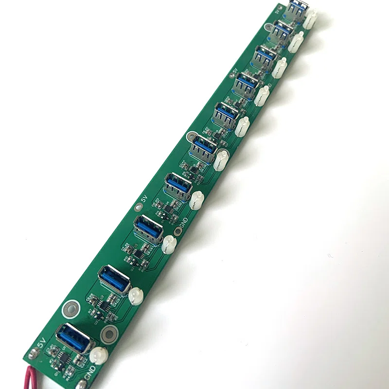
Surface-mount connectors, such as FPC, USB Type-C, and power cord terminals.
When designing interfaces, pay attention to the following:
Try to design independent grounding for each path (especially analog/digital shunts);
Ensure that adjacent interfaces do not interfere with each other, and add shielding GND if necessary;
Leave enough space for test points, voltage measurement, or troubleshooting;
It is recommended to equip each power supply with a decoupling capacitor to resist transient fluctuations.
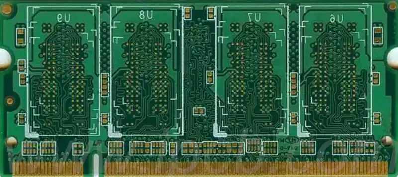
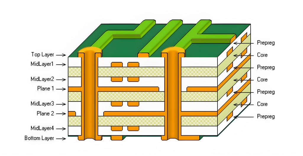
Multilayer board supported branch structure
For some applications with compact space and complex branching, such as electric vehicle control boards, industrial module controllers, etc., 4-layer or 6-layer PCB design can be used:
Top and bottom layers: I/O interfaces for connecting external modules;
Inner layer 1: main power supply line (12V/5V);
Inner layer 2: ground plane, as isolation and stability reference;
Connect each branch through blind/buried vias or current through holes.
Multilayer PCB can effectively reduce wiring complexity, improve signal integrity and enhance mechanical strength, but it also increases manufacturing costs and design thresholds.
Application cases and performance evaluation
Analysis of typical application scenarios
PCB splitters are widely used in various power management systems due to their simple structure, low cost and strong flexibility. The following are several common practical application scenarios:
Smart home appliance control board
In the control motherboard of smart air conditioners or washing machines, a 220V to 12V power module is often used to power the MCU main control, solenoid valve control module, display module, etc. By designing three branches on the PCB and connecting them to different functional modules, centralized power supply, clear wiring and easy maintenance are achieved.
Industrial Automation Equipment
In PLC or servo drive control systems, power input needs to be distributed with high precision according to module functions. For example, after the main control board receives 24V input, the onboard splitter is used to supply power to the logic unit, motor drive module and human-machine interface, and the fuse/TVS tube is used for overcurrent/overvoltage protection to improve system stability.
Automotive Power Module
In-vehicle control systems (such as ADAS and body controllers) often need to lead multiple power branches from the main wiring harness and distribute them to different subsystems through the PCB splitter structure, while using slots or ground partitions on the PCB board to improve electromagnetic compatibility.
Reliability test of shunt structure
Before electronic products leave the factory, the PCB shunt structure usually needs to pass a series of reliability tests to verify its electrical and mechanical performance:
Voltage drop test
Connect the maximum load to all output branches, monitor the voltage changes between the input and output ends, and ensure that the voltage drop is within an acceptable range (such as <5%).
Thermal stability test
Run for 2~4 hours under full load current conditions, measure the temperature rise of each branch with a thermal imager, and verify whether there are hot spots in the line or copper wire overheating.
EMI radiation test
High-frequency switching power supply systems often cause radiation interference. Evaluate the interference emission intensity of the PCB shunt structure to the outside world, and optimize the ground layout and increase the shielding structure as needed.
Plug-in reliability test
If the shunt output uses a plug/terminal connector, repeated plug-in and mechanical stress tests are also required to verify the firmness of the pad, solder joint fatigue and other issues.
Maintainability design of branch structure
In actual projects, a reasonable PCB splitter not only requires stable power supply, but also good maintainability and debugging convenience. The following are common auxiliary design methods:
Each output branch is equipped with a test point for voltage detection or oscilloscope probe access;
A fuse position or patch TVS is reserved for line protection;
DIP switches or jumpers are optional to control whether the branch is conductive, supporting flexible configuration;
The interface silk screen number is designed on the edge of the board to facilitate assembly and subsequent troubleshooting.
Technical challenges and future trend analysis
Current technical challenges
Although the design principle of PCB splitters seems simple, they still face many challenges in actual applications, especially in high-density, high-speed and high-power scenarios:
Space constraints and multi-branch conflicts
The size of modern electronic equipment is constantly shrinking, and the available board area is getting smaller and smaller. How to plan reasonable multi-channel outputs in a limited space to avoid cross wiring, electromagnetic interference and heat accumulation is a common problem for designers.
High-speed signal interference
Some power shunts not only transmit DC current, but also undertake data or high-frequency signal transmission tasks, such as USB-PD, PoE (Power over Ethernet), etc. This “power + signal” composite structure will bring signal integrity problems such as crosstalk and reflection, and put forward higher requirements for impedance control.
Difficulty of heat distribution and heat dissipation design
Especially in the fields of new energy vehicles and server power systems, the shunt structure bears tens of amperes of current, resulting in significant temperature rise in some lines. If the heat is concentrated in a single area, it will cause components to overheat or even be damaged. Therefore, how to combine shunt design with copper surface heat dissipation, thermal vias, metal substrates and other technologies is the key to improving reliability.
Safety regulations and isolation strategies are complicated
When a shunt needs to support both AC and DC outputs, or the main power supply and standby power supply coexist, the safety zone and functional zone must be strictly distinguished. Especially in industries involving strong electrical isolation such as medical, rail transit, and power adapters, strict requirements are placed on the width of the slots between boards, the spacing, and the withstand voltage path.
Optimization strategies to meet challenges
In response to the above problems, engineers and manufacturers have gradually proposed a variety of optimization solutions:
Differential wiring + local ground wrapping: suitable for high-speed data/power transmission design, reducing crosstalk and EMI;
Thick copper + multi-layer thermal via heat path: improve heat distribution efficiency and prevent local board burning;
Use ceramic substrate or aluminum substrate structure: for ultra-high power modules, improve heat dissipation efficiency and enhance mechanical strength;
Embedded modular plug-in solution: make the branch function into a plug-in module, and connect it to the main PCB through a pin header or edge connector to facilitate rapid maintenance and function expansion;
Intelligent controllable splitter design: introduce simple control logic, such as using MOS tube + MCU to control the on and off of each branch, to achieve software configuration, dynamic load switching and other functions.
Future development trends
With the continuous advancement of technology, PCB splitters will also present the following development directions in the future:
Integration with flexible circuits
In areas where the demand for flexible PCBs has surged, such as wearable devices and medical implants, traditional rigid splitting methods have gradually evolved towards flexibility and deformability, and the design needs to take into account both electrical performance and mechanical adaptability.
AI-assisted automatic splitting layout
With the help of AI layout tools, future designers can quickly obtain the optimal splitting path solution, make adaptive adjustments based on the load model, and improve development efficiency and wiring accuracy.
Digital twin technology supports predictive maintenance
Through the digital twin model, the operating status, temperature, and load changes of the splitter are simulated, and potential faults are monitored and predicted in real time, shifting from “passive maintenance” to “active management”.
Enhanced high-voltage/high-power compatibility
With the growing demand for charging piles, new energy, and industrial power supplies, the onboard splitting structure will support higher voltages and larger currents, while meeting global safety standards such as UL and CE.
Summary
Although small, PCB splitters play a key role in power management, signal distribution, and system stability. It not only simplifies the circuit structure, but also significantly improves the integration and maintainability of the product. As electronic equipment develops towards high density, high power and intelligence, PCB splitters are also evolving from simple wire distribution to intelligent, modular and predictable system nodes. For designers and manufacturers, understanding its structure, mastering its process and controlling its key indicators are an indispensable part of creating reliable electronic products.