The arrival of the Internet of Things era has directly promoted the rapid prosperity of Wide Area Low Power Networks (LPWANs) designed specifically for low bandwidth, low-power, long-distance, and large-scale connected IoT applications. In China, communication giants represented by Huawei and the three major telecommunications operators have taken the lead in targeting low-cost and wide coverage NB IoT in the field of wide area low-power consumption.
NB IoT has four major advantages: wide coverage, low power consumption, large connectivity, and low cost. In the field of small data volume and scattered data collection, it supplements the shortcomings of high energy consumption in 5G network technology and drives the development of edge analysis and computing in the Internet of Things. NB IoT has currently transitioned from 4G to 5G, with 5G technology divided into three segments: low-speed services (basic IoT connectivity), medium speed services (similar to 4G services), and high-speed services (autonomous driving, vehicle networking, remote healthcare, and video surveillance, etc.).
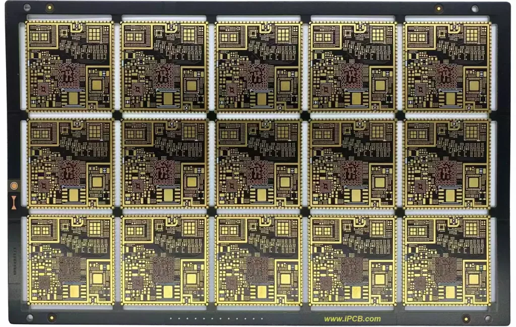
The early IoT module PCBs used a half hole method, and subsequent development needed to meet the needs of hot swapping, resulting in a gold finger type PCIe design. Due to the increase in I/O density, the bottom LGA design was developed, which used the LGA solder pads on the back to connect signals to the motherboard. PCB prototype come in pure bottom LGA design or LGA+half hole design on the PCB board edge.
With the development of 5G, the demand for signal transmission is becoming higher and higher. The selection of PCB materials has evolved from medium Tg materials to high Tg materials. In order to meet the high-speed signal transmission needs of 5G, Low Dk materials have been introduced. In the future, due to the requirements of higher I/O, faster signal transmission, low loss, and dimensional stability in high-density assembly, the application of BT materials and midloss materials will gradually increase. Due to the small module size, short wiring length, and the use of HDI blind hole design, the link loss is small, and materials at the midloss and BT levels can basically meet the requirements of the 5G high-speed section.
Design of IoT PCB
1.Stacking design of IoT PCBs
According to the functional requirements of integrated modules for IoT transmission, the design of 4-6 layer through-hole PCBs has gradually upgraded to integrate more functions and develop modularity, transitioning to HDI PCB, and from the original 1st order HDI PCB to 4th order HDI PCB, and gradually moving towards Anylayer. The development of 4G has reached the 5G stage, and this type of module is basically designed for HDI of order 3 or higher. The module board adopts high-density interconnection and integrates more and more functions; The motherboard can increase its area, reduce the number of stacked layers or HDI orders, and ultimately lower the overall packaging cost.
IoT PCB line width and line spacing (L/S) design
With the increasing demand for product transmission, the line width to line spacing (L/S) has evolved from an early 4/4mil or above to the current 3/3mil line width to line spacing, while the line capacity limit for traditional positive PCB production is 3/3mil. To meet the line width and line spacing (L/S) of less than 3/3mil, the current industry practices mostly use negative film vacuum etching and two fluid etching. Currently, the L/S mass production capacity of negative film vacuum etching process is 50/50 μ m, and the maximum vacuum etching capacity of adding two fluids is 40/40 μ m. With the increasingly higher requirements for product capability, the greater data processing and more functional integration of the Internet of Things and edge computing in the future, the Internet of Things module will go to the SLP process like the mobile phone motherboard in the future.
For IOT module PCBs, the PCIe interface module is designed with ordinary gold fingers or long and short gold fingers, and the technology is relatively mature; The difficulty of the bottom LGA design lies in the high-order HDI expansion and contraction, as well as the precise control of circuit yield. The machining process is simplified to a certain extent due to the disappearance of half holes. The IOT module with a half hole design, due to the relatively complex half hole production process, has multiple process options in the industry. Depending on whether the product actually requires half holes and the classification of circuit levels, the IoT PCB types and designed processes are different, which can be divided into two categories:
PCB design includes half hole type (L/S ≥ 3/3mil)
The module design includes half holes, and this type of board adopts a negative film process. After electroplating, the board is milled, and there is copper residue or the half hole mouth cannot be improved. To meet the product quality requirements, a positive film tin plating process is needed. The half hole mouth of the board is etched off through the etching method to improve the product quality. However, this method has circuit limitations (currently, the minimum positive film line width/line spacing capacity is 3/3mil). The IOT module with half hole design for fine circuits cannot meet the process capability of the positive circuit.
PCB design includes half hole type (L/S < 3/3mil)
At present, the etching capacity of the positive film in the industry is L/S ≥ 3/3mil, which exceeds the process capability requirements of the positive film process and can only be produced using negative films. Directly merging the half hole and forming in one go during the forming process simplifies the process and reduces production costs. However, the half hole cloak in this process has not been etched and cleaned of burrs, resulting in residual burrs and burrs on the hole wall during the milling process, which poses a quality issue.
Traditional low-end IoT module PCBs often adopt a half hole design, mainly used in 2G and 3G IOT applications, with fewer I/O quantities and a line width and line spacing of more than 3/3mil, which can meet the process of positive tin plating. As the product level increases and the line capacity becomes finer, adopting a positive film process cannot meet the requirements; However, in the negative film process, there may be burrs that cannot be removed. After the PCB is finished, solder burrs can easily lead to loose solder joints and virtual soldering, and in severe cases, it can cause two pin bridging short circuits, and even signal loss. Therefore, 4G and above products are designed using HDI PCB stacked production.
The structure of IoT PCB products has also changed from traditional half hole design to gold finger design and pure bottom LGA design, but some products will still use half hole+bottom LGA design. To meet actual production needs, the outer circuit design will require customers to choose a design line width/spacing of ≥ 3/3mil to meet production requirements.
At present, the Internet of Things has developed to 4G and above, and the line level is becoming increasingly refined, even reaching a line capacity level of 2mil. To improve the burr problem after milling half hole slots on negative films, it is necessary to reconsider the process and method improvement, in order to meet the manufacturing requirements of IoT module PCBs.