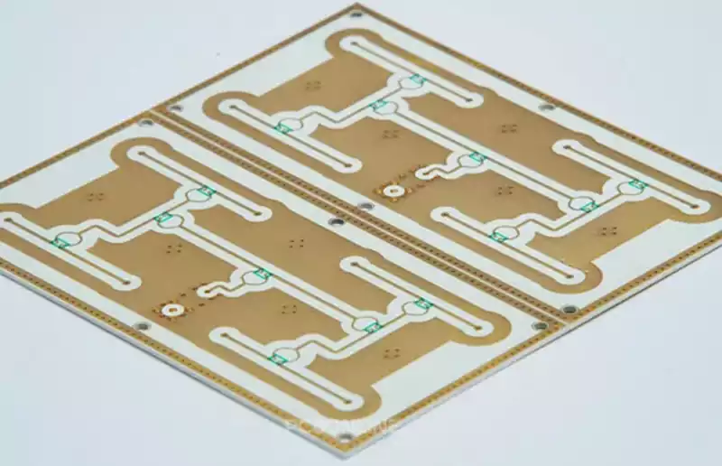
The pcb grounding plane on a PCB is typically a large metal area connected to the circuit ground. This metal area may only occupy a small portion of the board or, in multi-layer designs, it can span an entire layer. Depending on design requirements, it may even span multiple layers.
Grounding, in simple terms, is setting a ‘reference zero point’ for a circuit. The purpose of this ‘zero point’ is twofold: first, to provide a clear return path for current, and second, to stabilise circuit voltage and suppress noise interference. From a technical perspective, grounding involves establishing a low-impedance reference potential point, which is typically connected to the system’s common node or directly to a grounding rod.
However, pcb grounding is not limited to a single mode; it has multiple types, each with its unique functions and applicable scenarios:
Signal Ground: Signal ground provides a stable ‘reference line’ for analogue or digital signals, preventing signal drift. In most cases, signal ground and power ground are combined, but in some precision circuits with extremely high accuracy requirements, signal ground is set separately. Circuits with extremely high signal sensitivity, such as audio amplifiers, often utilise signal grounding.
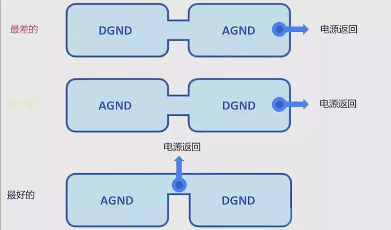
Power Ground: Power grounding handles the task of conducting high currents in the power circuit, ensuring stable power supply. Due to the high current flow, the power grounding path must be designed to be robust and sturdy; otherwise, voltage drops will occur when high currents pass through. Power grounding is commonly found in circuits that require high power, such as power modules and motor drives.
Safety Grounding: Safety grounding connects the equipment housing to the grounding system. In the event of a fault causing leakage current, it quickly diverts the current to prevent electric shock injuries. Safety grounding is typically directly connected to the earth and strictly adheres to safety standards. Household appliances and industrial equipment must all be equipped with safety grounding to ensure safe use.
Shield Grounding: Shield grounding involves grounding the shielding layer to block external electromagnetic interference. To avoid forming interference loops, shield grounding generally uses a single-point grounding method. In scenarios with high electromagnetic environment requirements, such as RF circuits and shielded cables, shield grounding plays a critical role.
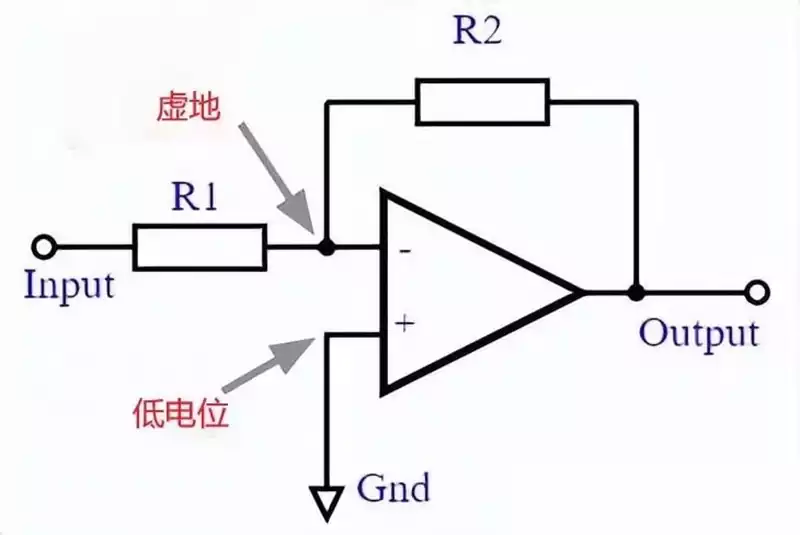
Virtual Ground: What is the function of a virtual ground? Taking an operational amplifier as an example, it has an ‘analog zero point’ internally. This ‘zero point’ is not actually connected to the earth, but its potential is the same as the actual zero point. A virtual ground is achieved through feedback control, and current does not flow through it. The concept of a virtual ground is frequently used in analog circuit design and amplifier performance analysis.
AC Ground: AC ground provides a stable reference potential for the power supply input terminal while effectively resisting high-frequency interference. It has low DC impedance and maintains stable potential even in high-frequency environments. AC ground is commonly used in circuits involving AC power conversion, such as switching power supplies and transformer circuits.
The ground plane on a PCB has three important purposes:
- Voltage return: Most components on a PCB are connected to the power network, and the return voltage is returned through the ground network. On boards with only one or two layers, the ground network typically requires wider traces for routing. However, by dedicating an entire layer to the ground plane on a multi-layer board, the process of connecting each component to the ground network is simplified.
- Signal return: Regular signals also need to return, and for high-speed designs, having a clear return path on the ground is very important. Without such a clear return path, these signals can cause significant interference to the rest of the PCB.
- Reducing Noise and Interference: As signal speeds increase, the switching states of digital circuits also become more frequent. This generates noise pulses through the grounding circuit, which may affect other parts of the circuit. A grounding layer with a larger conductive area helps reduce such interference because it has lower impedance compared to routing the grounding network via traces.
PCB Grounding Implementation Methods
PCB grounding can be implemented in various ways, primarily including single-point grounding, multi-point grounding, floating grounding, and hybrid grounding. Each grounding method has its own applicable scenarios and advantages/disadvantages, and designers must select the appropriate grounding strategy based on specific application requirements and circuit characteristics.
Single-Point Grounding:
Single-point grounding refers to a system where only one physical point is defined as the ground reference point, and all other points requiring grounding are directly connected to this point. This method is particularly effective in low-frequency circuits because the length of the conductors and parasitic effects have minimal impact at low frequencies. Single-point grounding reduces common-mode impedance coupling and low-frequency ground loop interference, but may introduce new issues in high-frequency circuits.
Multi-point grounding:
Multi-point grounding refers to connecting each grounding point in an electronic device directly to the nearest ground plane (such as the metal base plate of the device). This method is more common in high-frequency circuits because the effects of parasitic capacitance and inductance become significant at high frequencies. Multi-point grounding reduces interference caused by common ground impedance and minimises the impact of parasitic capacitance and inductance on signal integrity.
Floating ground:
Floating ground technology refers to a pcb grounding that is not directly connected to the earth via a conductor. This grounding method isolates the circuit from the electrical properties of the earth, providing a high isolation resistance between the power ground and signal ground, effectively blocking electromagnetic interference. However, floating ground is susceptible to the effects of parasitic capacitance, which may cause fluctuations in ground potential and increase induced interference in analogue circuits.
Mixed Grounding:
Mixed grounding is a compromise solution that combines the characteristics of single-point and multi-point grounding to accommodate different frequency requirements. In broadband-sensitive circuits, mixed grounding optimises performance by exhibiting different characteristics at low and high frequencies. For example, separating the DC ground from the RF ground via a capacitor prevents the formation of ground loops while maintaining low-impedance connections at high-frequency signal points.
PCB grounding is a fundamental yet complex art in electronic circuit design. It is not merely about providing a simple ‘zero potential’ reference but also concerns the effective return of current, system voltage stability, noise suppression, and optimisation of electromagnetic compatibility.