Ceramic antennas are not conventional ‘ceramic products’ but rather miniature antennas formed by integrating metal conductors (such as silver or copper) with ceramic dielectric materials through precision manufacturing processes. Their core principle leverages the propagation characteristics of electromagnetic waves within ceramic media: ceramic materials possess high dielectric constants and low loss properties, enabling significant reduction in antenna dimensions while maintaining signal transmission efficiency. For instance, aluminium nitride ceramics, valued for their high thermal conductivity and stable dielectric constant, find extensive application in high-frequency communication scenarios. Conversely, zirconia ceramics, prized for their exceptional strength, serve as the ideal choice for antennas in wearable devices.
Technologically, ceramic antenna manufacturing employs advanced processes including multilayer ceramic co-firing (LTCC) and laser direct structuring (LDS). Taking LTCC as an example, this technique involves forming ceramic powder into green tape, embedding circuit patterns during multilayer stacking, and finally co-firing at high temperatures to create three-dimensional antenna structures. This process not only achieves antenna miniaturisation (sizes can be reduced to one-third of traditional antennas) but also optimises frequency band coverage through multilayer design, meeting multi-mode communication requirements.
Constructed from ceramic materials, GPS ceramic antennas exhibit superior mechanical strength, enhanced wear resistance, and elevated temperature stability, ensuring reliable operation across diverse harsh environments. Furthermore, these antennas feature high precision, sensitivity, compact dimensions, and lightweight characteristics, facilitating seamless integration into various devices to deliver more intelligent functionality.
Key Considerations in GPS Ceramic Antenna Circuit Design
The circuit design for GPS ceramic antennas encompasses multiple critical aspects: antenna-to-receiver module interfacing, signal amplification and noise reduction, impedance matching, and power supply. Optimising these circuit elements ensures the efficient and stable operation of the GPS system.
Antenna Connection Circuit
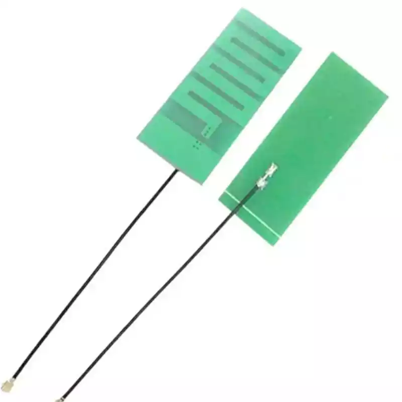
The antenna connection circuit establishes the physical and electrical link between the GPS ceramic antenna and the receiver module. Design considerations must fully account for the antenna’s impedance characteristics, operating frequency range, and the specific interface requirements of the receiver module. To guarantee signal transmission stability and interference resistance, coaxial cables are typically employed, or the antenna may be directly integrated onto the PCB. A meticulously designed antenna connection circuit ensures effective signal transfer from the antenna to the receiver module.
Low-Noise Amplifier (LNA) Circuit
The low-noise amplifier (LNA) circuit constitutes a core component in GPS ceramic antenna applications. Its primary function is to amplify the received weak GPS signals while effectively suppressing noise, thereby significantly enhancing the signal-to-noise ratio. During LNA circuit design, selecting high-performance amplifier chips is paramount, alongside precise calibration of their operating parameters. Additionally, attention must be paid to the amplifier chip’s power supply solution, impedance matching at input/output ports, and thermal management to guarantee circuit stability and optimal performance. As the core component of RF reception systems, low-noise amplifiers directly influence system sensitivity, dynamic range, and signal quality.
Impedance Matching Circuit
The impedance matching circuit is designed to adjust impedance differences between the antenna and the receiver module, ensuring signals are transmitted from the antenna to the receiver module with maximum efficiency and stability. When designing this circuit, appropriate matching components and circuit topologies must be selected based on the specific impedance characteristics of the antenna and the interface specifications of the receiver module. Furthermore, parameters such as the bandwidth and signal insertion loss of the matching circuit require careful consideration, as they directly impact the overall performance of the GPS system.
Power Management Circuit
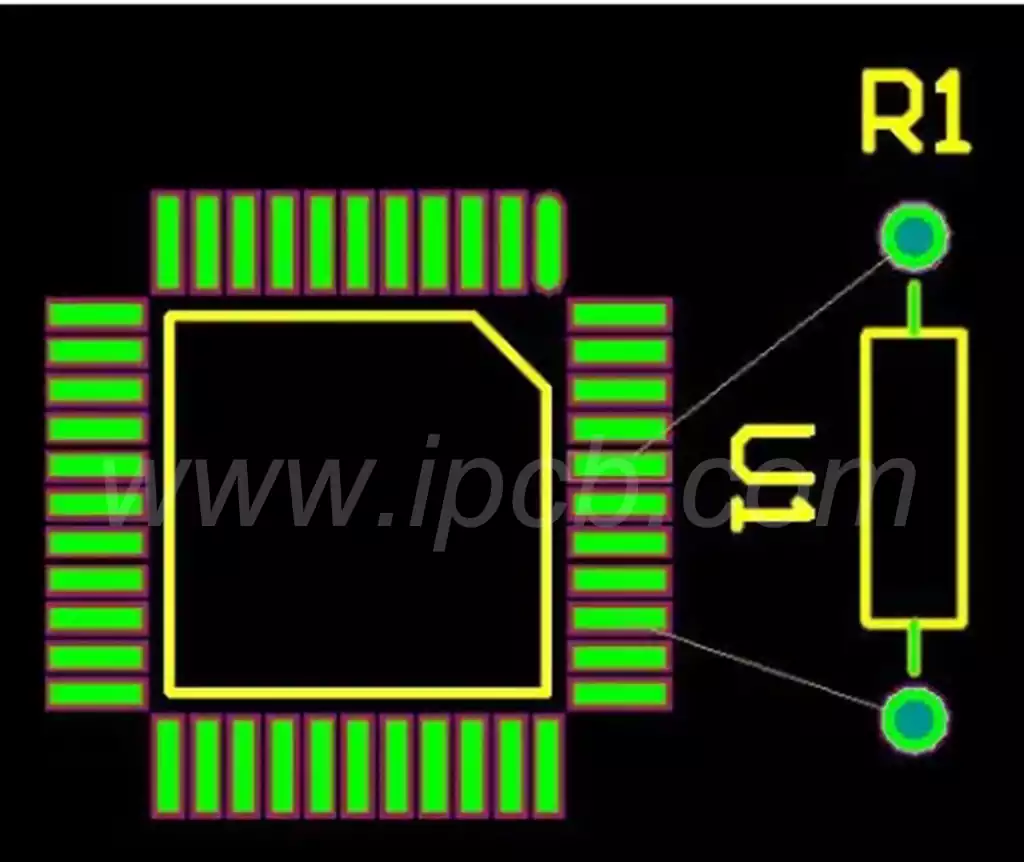
The power management circuit provides stable and reliable operating voltage and current for the entire application circuit of the GPS ceramic antenna. Design considerations must comprehensively address the power supply method, output voltage stability, ripple suppression capability, and thermal management requirements of the circuit. Selecting suitable power supply chips and power delivery strategies based on the circuit’s power consumption requirements is crucial for ensuring long-term system stability. For instance, routing should be avoided beneath the ceramic antenna, including power lines, as minute power supply noise may interfere with GPS signals. GPS modules frequently utilise ceramic planar antennas, typically augmented with external active amplification circuits.
Ceramic antennas demonstrate significant advantages in the communications field, particularly for GPS applications, owing to their unique material properties and advanced manufacturing techniques. Through scientific design, the high precision, sensitivity, and stable reliability of ceramic antennas can be fully leveraged, providing efficient and intelligent positioning solutions for diverse devices.